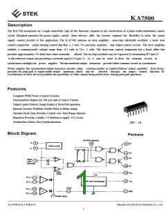
KA
7500
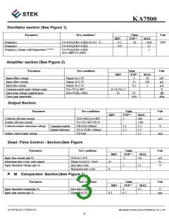
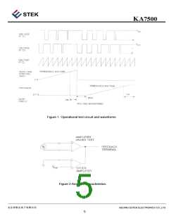
Oscillator section (See Figure 1)
Parameter
Test conditions*
Value
Unit
MIN
9.2
TYP**
MAX
10.8
12
Frequency
CT
CT
CT
=0.01µF,R
=0.01µF,R
=0.01µF,R
T
T
T
=12KΩ,T
=12KΩ
=12KΩ
A=25
°
C
10
-
kHz
Frequency
9.0
2
Frequency change with temperature *****
ΔTA=MIN TO MAX
Amplifier section (See Figure 2)
Parameter
Test conditions
Value
Unit
MIN
TYP*
2
MAX
10
Input offset voltage
Vo(pin 3)=2.5V
Vo(pin 3)=2.5V
Vo(pin 3)=2.5V
Vcc=7V to 40V
ΔVo=3V,RL=2KΩ,
mV
nA
µA
V
Input offset current
25
250
1
Input blas current
0.2
Common-mode input voltage range
Open-loop voltage amplification
Unity-gain bandwidth
-0.3 to Vcc-2
70
95
dB
kHz
650
Output Section
Parameter
Test conditions
Value
Unit
MIN
TYP**
MAX
Collector off-state current
Emitter off-state current
VCE=40V,Ccc=40V
Vcc=Vc=40V,VE=0
VE=0,Ic=200mA
VC=15V,IE=-200mA
VI=Vref
2
100
-100
1.3
µA
V
Collector-emitter saturation voltage
Common-emitter
Emitter-follower
1.1
1.5
2.5
Output control input current
3.5
mA
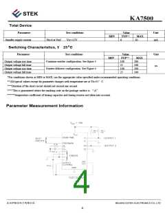
Dead -Time Control - Section(See Figure
Parameter
Test conditions
Value
TYP**
-2
Unit
MIN
MAX
Input bias current (pin 4)
VI=0 to 5.25V
-10
µA
%
Maximum duty cycle, each output
Input threshold voltage (pin 4)
VI(pin 4)=0,O.C.=Vref
Zero duty cycle
45
0
3
3.3
V
Maximum duty cycle
P M Comparator Section(See Figure 1)
Parameter
Test conditions
Value
TYP**
4
Unit
MIN
0.3
MAX
4.5
Input threshold voltage(pin 3)
Input sink current (pin 3)
Zero duty cycle
V(pin 3)=0.7V
V
0.7
mA
BEIJING ESTEK ELECTRONICS CO.,LTD
3

 ESTEK [ Estek Electronics Co. Ltd ]