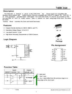
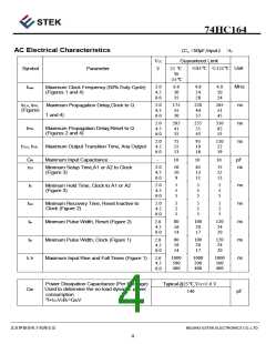
74HC164
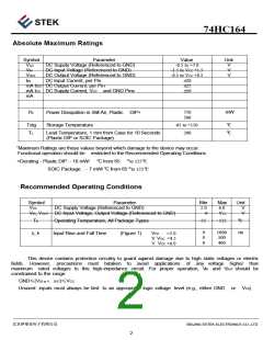
Absolute Maximum Ratings
Symbol
Parameter
Value
-0.5 to +7.0
-1.5 to VCC +1.5
-0.5 to VCC +0.5
Unit
V
V
V
V
V
CC
DC Supply Voltage (Referenced to GND)
DC Input Voltage (Referenced to GND)
DC Output Voltage (Referenced to GND)
DC Input Current, per Pin
IN
OUT
V
IIN
±
20
25
50
mA IOUT DC Output Current, per Pin
mA ICC DC Supply Current, VCC and GND Pins
mA
±
±
750
500
mW
P
D
Power Dissipation in Still Air, Plastic DIP+
Storage Temperature
Tstg
-65 to +150
260
C
C
T
L
Lead Temperature, 1 mm from Case for 10 Seconds
(Plastic DIP or SOIC Package)
*Maximum Ratings are those values beyond which damage to the device may occur.
Functional operation should be restricted to the Recommended Operating Conditions.
+Derating - Plastic DIP: - 10 mW/ C from 65 to 125°C
°
°
SOIC Package: : - 7 mW/ C from 65 to 125 C
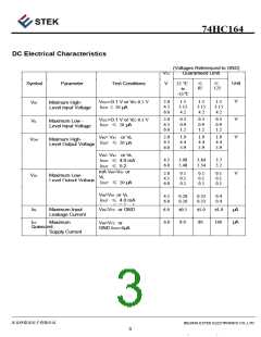
Recommended Operating Conditions
Symbol
Parameter
DC Supply Voltage (Referenced to GND)
Min
2.0
0
Max
6.0
Unit
V
VCC
VIN, VOUT DC Input Voltage, Output Voltage (Referenced to GND)
V
CC
V
T
A
Operating Temperature, All Package Types
-55
+125
°C
0
0
0
1000
500
400
ns
tr
, t
f
Input Rise and Fall Time
(Figure 1)
V
V
V
CC
=2.0
CC =4.5
CC =6.0
V
V
This device contains protection circuitry to guard against damage due to high static voltages or electric
fields. However, precautions must betaken to avoid applications of any voltage higher than
maximum rated voltages to this high-impedance circuit. For proper operation, VIN and VOUT should be
constrained to the range
GND≤(VIN or V OUT)≤VCC.
Unused inputs must always be tied to an appropriate logic voltage level (e.g., either GND or
V
CC).
BEIJING ESTEK ELECTRONICS CO.,LTD
2

 ESTEK [ Estek Electronics Co. Ltd ]