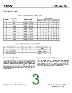
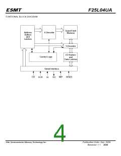
ESMT
F25L04UA
Instructions
Instructions are used to Read, Write (Erase and Program), and
configure the F25L04UA. The instruction bus cycles are 8 bits
each for commands (Op Code), data, and addresses. Prior to
executing any Byte-Program, Auto Address Increment (AAI)
programming, Sector-Erase, Block-Erase, or Chip-Erase
instructions, the Write-Enable (WREN) instruction must be
executed first. The complete list of the instructions is provided in
Table 5. All instructions are synchronized off a high to low
SCK starting with the most significant bit. CE must be driven
low before an instruction is entered and must be driven high after
the last bit of the instruction has been shifted in (except for Read,
Read-ID and Read-Status-Register instructions). Any low to high
transition on CE , before receiving the last bit of an instruction
bus cycle, will terminate the instruction in progress and return the
device to the standby mode.
Instruction commands (Op Code), addresses, and data are all
input from the most significant bit (MSB) first.
transition of CE . Inputs will be accepted on the rising edge of
TABLE 5: DEVICE OPERATION INSTRUCTIONS
Max
Freq
MHz
Bus Cycle4
Cycle Type/
Operation1,2
1
2
3
4
5
6
SIN
SOUT
SIN
SOUT
SIN
SOUT
SIN
SOUT SIN SOUT SIN
SOUT
Read
33
03H
0BH
20H
60H
02H
Hi-Z A23-A16 Hi-Z A15-A8 Hi-Z A7-A0 Hi-Z
Hi-Z A23-A16 Hi-Z A15-A8 Hi-Z A7-A0 Hi-Z
Hi-Z A23-A16 Hi-Z A15-A8 Hi-Z A7-A0 Hi-Z
X
X
-
DOUT
X
-
High-Speed-Read
X
DOUT
Sector-Erase4,5
Chip-Erase6
Hi-Z
-
-
-
-
-
-
-
-
Byte-Program5
Hi-Z A23-A16 Hi-Z A15-A8 Hi-Z A7-A0 Hi-Z DIN
Hi-Z
Hi-Z
50
and
75
Auto Address Increment
(AAI) Single-Byte Program5,6
Read-Status-Register
(RDSR)
AFH Hi-Z A23-A16 Hi-Z A15-A8 Hi-Z A7-A0 Hi-Z DIN
05H
50H
01H
Hi-Z
Hi-Z
Hi-Z
X
-
DOUT
-
-
-
Note7
-
-
-
Note7
-
-
-
Note7
-
Enable-Write-Status-Register
and
100
(EWSR)8
Write-Status-Register
(WRSR)8
Write-Enable (WREN)
Write-Disable (WRDI)
Jedec-Read-ID (JEDEC-ID)
Data
Hi-Z
-
-
-
-
-
-.
-
-
-
-
-
-
-
06H
04H
9FH
Hi-Z
Hi-Z
Hi-Z
-
-
X
8CH
X
8CH
X
8CH
-
-
1. Operation: SIN = Serial In, SOUT = Serial Out
2. X = Dummy Input Cycles (VIL or VIH); - = Non-Applicable Cycles (Cycles are not necessary)
3. One bus cycle is eight clock periods.
4. Sector addresses: use AMS-A12, remaining addresses can be VIL or VIH
5. Prior to any Byte-Program, AAI-Program, Sector-Erase ,or Chip-Erase operation, the Write-Enable (WREN) instruction must be
executed.
6. To continue programming to the next sequential address location, enter the 8-bit command, AFH, followed by the data to be
programmed.
7. The Read-Status-Register is continuous with ongoing clock cycles until terminated by a low to high transition on CE .
8. The Enable-Write-Status-Register (EWSR) instruction and the Write-Status-Register (WRSR) instruction must work in conjunction
of each other. The WRSR instruction must be executed immediately (very next bus cycle) after the EWSR instruction to make both
instructions effective.
9. The Jedec-Read-ID is continuous with on going clock cycles until terminated by a low to high transition on CE .
Elite Semiconductor Memory Technology Inc.
Publication Date: Sep. 2006
Revision: 1.1 7/24

 ESMT [ ELITE SEMICONDUCTOR MEMORY TECHNOLOGY INC. ]