Limited Internal
E
ESKEVIN
PRODUCT SPECIFICATION
2 (5)
Prepared (also subject responsible if other)
No.
2/1301-BMR 637 02/94 Uen
147
Technical Specification
Approved
Checked
Date
Rev
EN/LZT 146 3R0e6feRre4nAceJuly 2008
PKM 4000D PINB Series
SEC/D (Julia You)
EYINGJI
2007-12-17
D
© Ericsson Power Modules AB
DC/DC converters, Input 36-75 V, Output 40 A/132 W
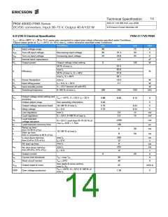
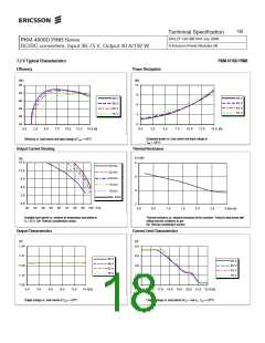
7.2 V Electrical Specification
PKM 4116D PINB
Tref = -40 to +90ºC, VI = 36 to 75 V, unless otherwise specified under Conditions.
Typical values given at: Tref = +25°C, VI= 53 V, max IO , unless otherwise specified under Conditions.
Characteristics
Conditions
min
36
typ
max
Unit
V
VI
Input voltage range
75
VIoff
VIon
CI
Turn-off input voltage
Turn-on input voltage
Internal input capacitance
Output power
Decreasing input voltage
Increasing input voltage
31
34
V
V
4.3
μF
W
PO
Output voltage initial setting
f = 100 Hz sinewave, 1 Vp-p
50 % of max IO
0
108
SVR
Supply voltage rejection (ac)
60
dB
92.6
91.6
92.8
91.5
max IO , VI = 53 V ,Tref = +25°C
50 % of max IO , VI = 48 V
max IO , VI = 48 V
91
η
Efficiency
%
Pd
Pli
Power Dissipation
Input idling power
Input standby power
Switching frequency
max IO, VI = 53 V ,Tref = +25°C
IO= 0, VI = 53 V
10.7
W
W
1.8
108
200
PRC
fs
VI = 53 V (turned off with RC)
0 -100% of max IO
mW
kHz
180
220
Output voltage initial setting and
accuracy
7.06
7.34
V
T
ref = +25°C, VI = 53 V, IO = max IO Vadj,
VOi
see Note 1
Output adjust range
Output voltage tolerance band
Idling voltage
6.48
6.99
6.99
7.92
7.41
7.41
20
V
V
10-100% of max IO
IO = 0
V
VO
Line regulation
max IO
mV
mV
Load regulation
VI = 53 V, 1-100% of max IO
10
Load transient
voltage deviation
VI = 53 V, Load step 25-75-25 % of max IO,
di/dt = 1 A/μs,
see Note 2
Vtr
ttr
tr
±340
135
7
mV
us
Load transient recovery time
Ramp-up time
(from 10−90 % of VOi)
4
25
ms
10-100% of max IO
Start-up time
(from VI connection to 90% of VOi)
ts
5
0
9
25
15
ms
IO
Output current
A
A
A
Ilim
Isc
Current limit threshold
Short circuit current
Vo =6.48 V, Tref < max Tref
17
21
Tref = 25ºC, VO = < VOnom * 0.1
See ripple & noise section,
max IO, VO.
VOac
OVP
Output ripple & noise
35
70
mVp-p
V
Tref = +25°C, VI = 53 V, IO = 0-100% of
max IO
Over Voltage Protection
9.5
Note 1: When using Vadj function, max output power (PO) must not be exceeded
Note 2: Output filter according to Ripple & Noise section

 ERICSSON [ ERICSSON ]