epc3xx
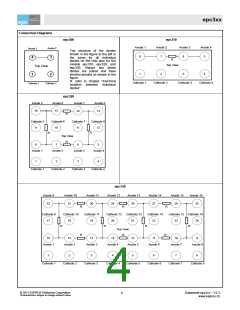
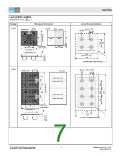
Layout Information
(all measures in mm,
)
Package
Mechanical Dimensions
Layout Recommendations
CSP4
0.14
max 0.10
0.10
max. 0.1524
Bottom View
Top View
∅ 0.30
4
1
3
2
photo diode
area
photo diode
area
0.40
0.50
Solder balls
Sn97.5Ag2.5
1.00 +0.00/-0.10
photosensitive area
0.50
1.00
no solder mask inside this area
CSP8
0.14
max. 0.1524
Bottom View
Top View
∅ 0.30
photo diode area
photo diode area
photo diode area
photo diode area
0.50
Solder balls
Sn97.5Ag2.5
1.00 ±0.00/-0.10
photosensitive area
0.50
1.00
no solder mask inside this area
© 2011 ESPROS Photonics Corporation
Characteristics subject to change without notice
7
Datasheet epc3xx - V2.3
www.espros.ch

 EPC [ ESPROS PHOTONICS CORP ]