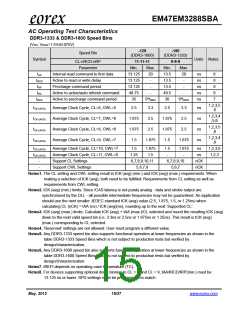
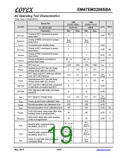
EM47EM3288SBA
AC Operating Test Characteristics
DDR3-1333 & DDR3-1600 Speed Bins
(VDD, VDDQ=1.5V±0.075V)
-125
(DDR3-1600)
-150
(DDR3-1333)
Speed Bin
Symbol
Units Notes
CL-nRCD-nRP
11-11-11
9-9-9
Parameter
Min.
13.125
13.125
13.125
48.75
35
Max.
Min.
13.5
13.5
13.5
49.5
36
Max.
tAA
tRCD
tRP
Internal read command to first data
Active to read or write delay
20
20
ns
ns
ns
ns
ns
8
8
8
8
7
-
-
Precharge command period
-
-
-
-
tRC
Active to active/auto refresh command
Active to precharge command period
tRAS
9*tREFI
9*tREFI
1,2,3,5
.6
tCK (AVG)
tCK (AVG)
tCK (AVG)
tCK (AVG)
Average Clock Cycle, CL=6, CWL=5
Average Clock Cycle, CL=7, CWL=6
Average Clock Cycle, CL=8, CWL=6
Average Clock Cycle, CL=9, CWL=7
2.5
1.875
1.875
1.5
3.3
2.5
2.5
1.875
1.875
1.5
3.3
2.5
ns
ns
ns
ns
1,2,3,4
,5,6
1,2,3,5
,6
2.5
2.5
1,2,3,4
,6
1.875
1.875
tCK (AVG)
Average Clock Cycle, CL=10, CWL=7
Average Clock Cycle, CL=11, CWL=8
Support CL Settings
1.5
1.875
1.5
1.5
-
1.875
-
ns
ns
1,2,3,6
1,2,3
tCK (AVG)
1.25
-
-
6,7,8,9,10,11
5,6,7,8
6,7,8,9,10
5,6,7
nCK
nCK
Support CWL Settings
Notes1. The CL setting and CWL setting result in tCK (avg) (min.) and tCK (avg) (max.) requirements. When
making a selection of tCK (avg), both need to be fulfilled: Requirements from CL setting as well as
requirements from CWL setting.
Notes2. tCK (avg) (min.) limits: Since /CAS latency is not purely analog - data and strobe output are
synchronized by the DLL - all possible intermediate frequencies may not be guaranteed. An application
should use the next smaller JEDEC standard tCK (avg) value (2.5, 1.875, 1.5, or 1.25ns) when
calculating CL (nCK) = tAA (ns) / tCK (avg)(ns), rounding up to the next ‘Supported CL’.
Notes3. tCK (avg) (max.) limits: Calculate tCK (avg) + tAA (max.)/CL selected and round the resulting tCK (avg)
down to the next valid speed bin (i.e. 3.3ns or 2.5ns or 1.875ns or 1.25ns). This result is tCK (avg)
(max.) corresponding to CL selected.
Notes4. ‘Reserved’ settings are not allowed. User must program a different value.
Notes5. Any DDR3-1333 speed bin also supports functional operation at lower frequencies as shown in the
table DDR3-1333 Speed Bins which is not subject to production tests but verified by
design/characterization.
Notes6. Any DDR3-1600 speed bin also supports functional operation at lower frequencies as shown in the
table DDR3-1600 Speed Bins which is not subject to production tests but verified by
design/characterization.
Notes7. tREFI depends on operating case temperature (TC).
Notes8. For devices supporting optional down binning to CL = 7 and CL = 9, tAA/tRCD/tRP(min.) must be
13.125 ns or lower. SPD settings must be programmed to match.
May. 2012
15/37
www.eorex.com

 EOREX [ EOREX CORPORATION ]