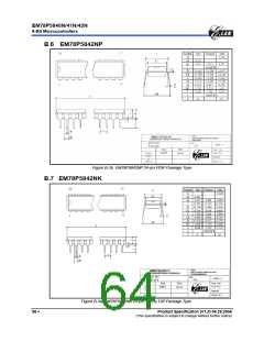
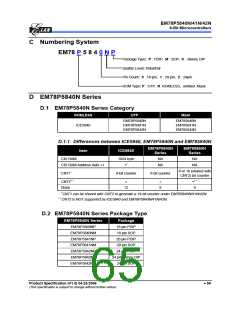
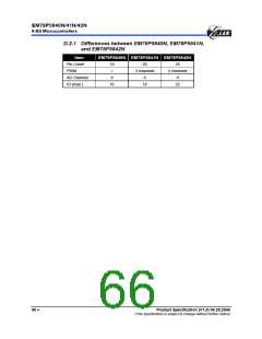
EM78P5840N/41N/42N
8-Bit Microcontrollers
E Application Notes
1. There are some undefined or not existing bits in the registers. User needs to be
cautious in dealing with those bits while programming and should not use them as
data to execute logic or math operations, since those bits have no relative functions
and have never been tested. Different symbols are used to distinguish them.
“0” or “1” → value always equal to 0 or value always equal to 1, (not existent, read
only)
“-“
→ value unknown, (not existent) undefined bits are not allowed for use.
2. You will notice that most of the register bit number, name, type, etc., are shown in
table format in this specification. The following are the conventions used to
describe the entry in each row and column in the table.
RA
PAGE0
Bit 5
BAB5
R-1
Bit 0
RAB0
R/W
Bit 6
RAB6
R/W-0
Bit 4
Bit 3
-
Bit 2
RAB2
R
Bit 1
RAB1
R-0
Bit 7
RAB7
R/W-0
RAB4
R/W-1
read/write
(default value=1)
read/write
(w/o default value)
read/write
(default value=0)
read only
(w/o default value)
Bit type
Bit name
(undefined) not allowed to use
Bit number
read only
(default value=1)
read only
(default value=0)
Register name and its page
3. Always set IOCC PAGE1 Bit 0 = 1, otherwise partial ADC function cannot be used.
4. Do NOT switch the MCU operation mode from Normal mode to Sleep mode directly.
Before going into Idle or Sleep mode, switch the MCU to Green mode first.
5. While switching the main clock (regardless whether from high freq to low freq or
vice versa), adding six instruction delay (NOP) is required.
6. The offset voltage will affect the ADC result. See Figure 10-3 in Section 10-2 for
details.
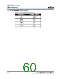
7. Do NOT connect unnecessary circuits on the OTP burner pins during the burning
process of the OTP ROM.
8. For low pin count package, some pins do not appear on package, but they exist on
dies. Do NOT keep these unused pins floating. Set these pins output to high or
low.
Product Specification (V1.0) 04.25.2006
(This specification is subject to change without further notice)
• 61

 ELAN [ ELAN MICROELECTRONICS CORP ]