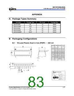
EM78P259N/260N
8-Bit Microprocessor with OTP ROM
/RESET= 'High', Fosc=32kHz
(Crystal type,CLKS="0"), output
pin floating, WDT enabled
Operating supply current
at two clocks (VDD to 3V)
ICC2
ICC3
ICC4
15
25
µA
mA
mA
/RESET= 'High', Fosc=4MHz
(Crystal type, CLKS="0"), output
pin floating, WDT enabled
Operating supply current
at two clocks
1.9
3.0
2.2
3.5
/RESET= 'High', Fosc=10MHz
(Crystal type, CLKS="0"), output
pin floating, WDT enabled
Operating supply current
at two clocks
NOTE: 1. These parameters are hypothetical (not tested) and are provided for design reference use only.
2. Data under minimum, typical, & maximum (Min, Typ, & Max) columns are based on hypothetical
results at 25℃. These data are for design reference only.
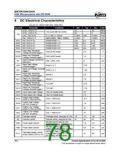
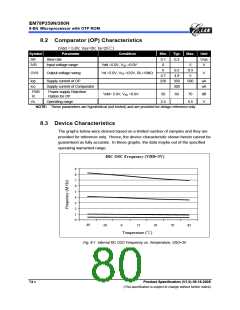
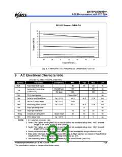
8.1 AD Converter Characteristics
(Vdd=2.5V to 5.5V, Vss=0V, Ta=25℃)
Symbol
VAREF
VASS
Parameter
Analog reference voltage
Analog input voltage
Analog supply current
Condition
VAREF - VASS≧2.5V
–
Min.
2.5
Typ.
–
Max.
Vdd
Vss
Unit
V
Vss
VASS
750
–10
500
200
–
V
VAI
–
VAREF
1000
+10
V
Ivdd
IAI1
850
0
uA
uA
uA
uA
Vdd=VAREF=5.0V, VASS =0.0V
(V referenced from Vdd)
Ivref
Ivdd
IAI2
600
250
820
Vdd=VAREF=5.0V, VASS=0.0V
(V referenced from VREF)
Analog supply current
OP current
IVref
300
Vdd=5.0V, OP used
IOP
450
550
650
uA
Output voltage swing 0.2V to
4.8V
RN
LN
Resolution
Vdd=VAREF=5.0V, VASS =0.0V
Vdd = 2.5 to 5.5V Ta=25℃
Vdd = 2.5 to 5.5V Ta=25℃
Vdd=VAREF=5.0V, VASS =0.0V
Vdd=VAREF=5.0V, VASS =0.0V
10
0
11
±4
–
±8
Bits
LSB
LSB
LSB
LSB
Linearity error
DNL
FSE
OE
Differential nonlinear error
Full scale error
Offset error
0
±0.5
±4
±0.9
±8
±0
±0
±2
±4
Recommended impedance of
analog voltage source
ZAI
–
0
8
10
KΩ
TAD
TCN
ADIV
ADC clock period
Vdd=VAREF=5.0V, VASS =0.0V
Vdd=VAREF=5.0V, VASS =0.0V
4
15
0
–
–
–
15
us
TAD
V
AD conversion time
ADC OP input voltage range Vdd=VAREF=5.0V, VASS =0.0V
–
VAREF
0.3
5
0
0.2
4.8
0.3
–
Vdd=VAREF=5.0V, VASS =0.0V,
ADC OP output voltage swing
ADOV
V
RL=10KΩ
4.7
0.1
±0
ADSR
PSR
ADC OP slew rate
Vdd=VAREF=5.0V, VASS =0.0V
Vdd=5.0V±0.5V
–
V/us
LSB
Power Supply Rejection
±2
NOTE: 1. These parameters are hypothetical (not tested) and are provided for design reference use only.
2. There is no current consumption when ADC is off other than minor leakage current.
3. AD conversion result will not decrease when an increase of input voltage and no missing code will
result.
Product Specification (V1.0) 06.16.2005
• 73
(This specification is subject to change without further notice)

 ELAN [ ELAN MICROELECTRONICS CORP ]