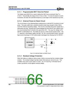
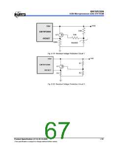
EM78P258N
8-Bit Microprocessor with OTP ROM
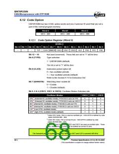
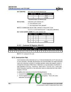
Bit 7 (WDTPS):
WDT time-out Period Selection bit
WDT Time
WDT time-out Period *
1
0
18 ms
4.5 ms
*Theoretical values, for reference only
Bit 6 (CYES):
Instruction cycle selection bit
0 = one instruction cycle.
1 = two instructions cycle (default)
Bit 5, 4, 3, & Bit 2 (C3, C2, C1, C0): Calibrator of internal RC mode
C3, C2, C1, & C0 must be set to “1” only (auto-calibration).
Bit 1 & Bit 0 (RCM1, RCM0): RC mode selection bits
RCM 1
RCM 0
Frequency (MHz)
1
1
0
0
1
0
1
0
4
8
1
455kHz
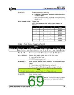
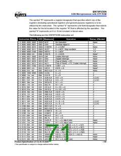
6.12.3 Customer ID Register (Word 2)
WORD 2
Bit 12 Bit 11 Bit 10 Bit 9 Bit 8 Bit 7 Bit 6 Bit 5 Bit 4 Bit 3 Bit 2 Bit 1 Bit 0
X
X
X
X
X
X
X
X
X
X
X
X
X
Bit 12 ~ 0 : Customer’s ID code
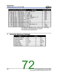
6.13 Instruction Set
Each instruction in the instruction set is a 13-bit word divided into an OP code and one
or more operands. Normally, all instructions are executed within one single instruction
cycle (one instruction consists of 2 oscillator periods), unless the program counter is
changed by instructions "MOV R2,A," "ADD R2,A," or by instructions of arithmetic or
logic operation on R2 (e.g., "SUB R2,A," "BS(C) R2,6," "CLR R2," etc.). In this case,
these instructions need one or two instruction cycles as determined by Code Option
Register CYES bit.
In addition, the instruction set has the following features:
1. Every bit of any register can be set, cleared, or tested directly.
2. The I/O registers can be regarded as general registers. That is, the same
instruction can operate on I/O registers.
64 •
Product Specification (V1.0) 06.16.2005
(This specification is subject to change without further notice)

 ELAN [ ELAN MICROELECTRONICS CORP ]