EL400C
200MHz Current Feedback Amplifier
Applications Information
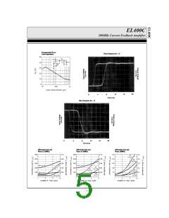
measurement is then made with a 0.714V DC offset
(100IRE). Differential Gain is a measure of the change
in amplitude of the sine wave, and is measured in per-
cent. Differential Phase is a measure of the change in
phase, and is measured in degrees. Typically, the maxi-
mum positive and negative deviations are summed to
give peak values.
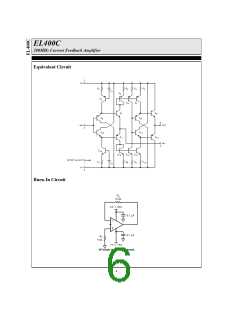
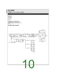
Theory of Operation
The EL400C has a unity gain buffer from the non-invert-
ing input to the inverting input. The error signal of the
EL400C is a current flowing into (or out of) the inverting
input. A very small change in current flowing through the
inverting input will cause a large change in the output
voltage. This current amplification is called the trans-
impedance (ROL) of the EL400C [VOUT=(ROL)*(-IIN)].
Since ROL is very large, the current flowing into the
inverting input in the steady-state (non-slewing) condi-
tion is very small.
In general, a back terminated cable (75W in series at the
drive end and 75W to ground at the receiving end) is pre-
ferred since the impedance match at both ends will
absorb any reflections. However, when double-termina-
tion is used, the received signal is reduced by half;
therefore a gain of 2 configuration is typically used to
compensate for the attenuation. In a gain of 2 configura-
tion, with output swing of 2VPP, with each back-
terminated load at 150W. The EL400C is capable of
driving up to 4 back-terminated loads with excellent
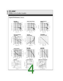
video performance. Please refer to the typical curves for
more information on video performance with respect to
frequency, gain, and loading.
Therefore we can still use op-amp assumptions as a first-
order approximation for circuit analysis, namely that:
1. The voltage across the inputs is approximately 0V.
2. The current into the inputs is approximately 0mA.
Resistor Value Selection and Optimization
The value of the feedback resistor (and an internal
capacitor) sets the AC dynamics of the EL400C. The
nominal value for the feedback resistor is 250W, which
is the value used for production testing. This value guar-
antees stability. For a given closed-loop gain the
bandwidth may be increased by decreasing the feedback
resistor and, conversely, the bandwidth may be
decreased by increasing the feedback resistor.
Capacitive Feedback
The EL400C relies on its feedback resistor for proper
compensation. A reduction of the impedance of the feed-
back element results in less stability, eventually
resulting in oscillation. Therefore, circuit implementa-
tions which have capacitive feedback should not be used
because of the capacitor's impedance reduction with fre-
quency. Similarly, oscillations can occur when using the
technique of placing a capacitor in parallel with the feed-
back resistor to compensate for shunt capacitances from
the inverting input to ground.
Reducing the feedback resistor too much will result in
overshoot and ringing, and eventually oscillations.
Increasing the feedback resistor results in a lower -3dB
frequency. Attenuation at high frequency is limited by a
zero in the closed-loop transfer function which results
from stray capacitance between the inverting input and
ground. Consequently, it is very important to keep stray
capacitance to a minimum at the inverting input.
Offset Adjustment Pin
Output offset voltage of the EL400C can be nulled by
tying a 10k potentiometer between +VS and -VS with the
slider attached to pin 1. A full-range variation of the
voltage at pin 1 to ±5V results in an offset voltage
adjustment of at least ±10mV. For best settling perfor-
mance pin 1 should be bypassed to ground with a
ceramic capacitor located near to the package, even if
the offset voltage adjustment feature is not being used.
Differential Gain/Phase
An industry-standard method of measuring the distor-
tion of a video component is to measure the amount of
differential gain and phase error it introduces. To mea-
sure these, a 40 IREPP reference signal is applied to the
device with 0V DC offset (0IRE) at 3.58MHz for NTSC,
4.43MHz for PAL, and 30MHz for HDTV. A second
7

 ELANTEC [ ELANTEC SEMICONDUCTOR ]