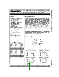
EL2210C/11C, EL2310C/11C, EL2410C/11C
Low Cost, Dual, Triple and Quad Video Op Amps
Absolute Maximum Ratings (T = 25°C)
A
Total Voltage Supply
18V
Power Dissipation
See Curves
-65°C to +150°C
-40°C to +85°C
+150°C
Input Voltage
±VS
6V
Storage Temperature Range
Operating Temperature Range
Die Junction Temperature
Differential Input Voltage
Peak Output Current
75mA (per amplifier)
Important Note:
All parameters having Min/Max specifications are guaranteed. Typ values are for information purposes only. Unless otherwise noted, all tests are at the
specified temperature and are pulsed tests, therefore: TJ = TC = TA.
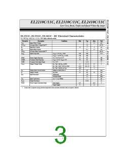
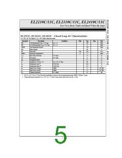
EL2210C, EL2310C, EL2410C - DC Electrical Characteristics
VS = ±5V, RL = 1kW, TA = 25°C unless otherwise noted.
Parameter
VOS
Description
Input Offset Voltage
Conditions
Min
Typ
10
Max
20
Unit
mV
EL2310C only
EL2311C only
10
25
mV
5
25
mV
TCVOS
IB
Average Offset Voltage Drift [1]
Input Bias Current
-25
-7
µV/°C
µA
-15
-3
IOS
Input Offset Current
0.5
1.5
µA
TCIOS
AVOL
Average Offset Current Drift [1]
-7
nA/°C
V/V
Open-Loop Gain
VOUT = ±2V, RL = 1kW
VOUT = +2V/0V, RL = 150W
VS = ±4.5V to ±5.5V
VCM = ±2.4V, VOUT = 0V
VS = ±5V
160
160
50
250
250
60
PSRR
CMRR
CMIR
VOUT
Power Supply Rejection
Common Mode Rejection
Common Mode Input Range
Output Voltage Swing
dB
dB
V
60
80
-5/+3
-3, 3
-0.6, 2.9
RL = RF= 1kW RL to GND
RL = RF = 1kW +150¾ to GND
RL = RF = 1kW RL to VEE
Output to GND (Note 1)
No Load (per channel)
Differential
-2.5
-0.45
-4.95
75
2.7
2.5
3
V
ISC
IS
Output Short Circuit Current
Supply Current
125
6.8
mA
mA
kW
MW
pF
5.5
10
RIN
Input Resistance
150
1.5
Common Mode
CIN
Input Capacitance
AV = +1 @ 10MHz
1
ROUT
PSOR
Output Resistance
0.150
W
Power Supply Operating Range
Dual Supply
±4.5
9
±6.5
13
V
Single Supply
1. A heat-sink is required to keep junction temperature below absolute maximum when an output is shorted
2

 ELANTEC [ ELANTEC SEMICONDUCTOR ]