EL2003C, EL2033C
100MHz Video Line Driver
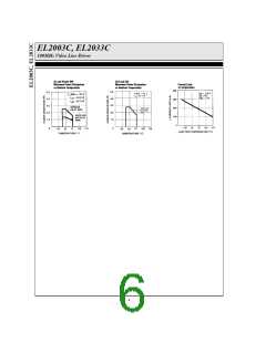
The thermal resistance junction to case is 50°C/W for
the plastic DIP. A suitable heat sink will increase the
power dissipation capability significantly beyond that of
the package alone. Several companies make standard
heat sinks for both packages. Aavid and Thermalloy heat
sinks have been used successfully.
formed by the device output resistance and the load
resistance.
R
L
A
= 0.995 ´ ------------------------------
V
R
+ R
L
OUT
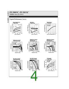
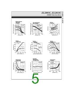
The high frequency response of the EL2003C and
EL2033C varies with the value of the load resistance as
shown in the characteristic curves. If the 100MHz peak-
ing is undesirable when driving load resistors greater
than 50W, an RC snubber circuit can be used from the
output to ground. The snubber circuit works by present-
ing a high frequency load resistance of less than 50W
while having no loading effect at low frequencies.
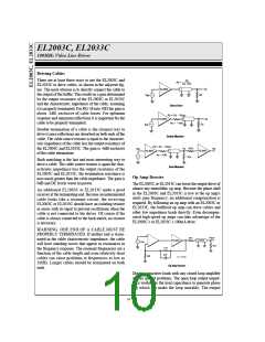
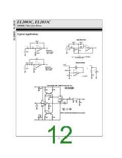
Parallel Operation
If more than 100mA output is required or if heat man-
agement is a problem, several EL2003C or EL2033Cs
may be paralleled together. The result is as though each
device was driving only part of the load. For example, if
two units are paralleled then a 50W load looks like 100W
to each EL2003C. Parallel operation results in lower
input and output impedances, increased bias current but
no increase in offset voltage. An example showing three
EL2003Cs in parallel and also the addition of a FET
input buffer stage is shown below. By using a dual FET
the circuit complexity is minimal and the performance is
excellent. Take care to minimize the stray capacitance at
the input of the EL2003Cs for maximum slew rate and
bandwidth.
Small Signal Response
Parallel Operation
I
³ ±300 mA
OUT
R
OUT
2W
BW 100MHz
SR = 1000V/µs
R
L
= 50W, C = 10pF, V = ±15V
L S
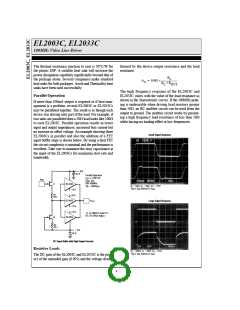
Top is V , Bottom is V
IN
OUT
Large Signal Response
J1, J2 2N5911 Dual FET
R1, R2 Offset Adjust
FET Input Buffer with High Output Currents
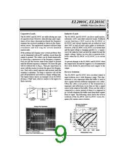
Resistive Loads
R
L
= 100W, C = 10pF, V = ±15V
L S
Top is V , Bottom is V
IN
OUT
The DC gain of the EL2003C and EL2033C is the prod-
uct of the unloaded gain (0.995) and the voltage divider
8

 ELANTEC [ ELANTEC SEMICONDUCTOR ]