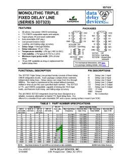
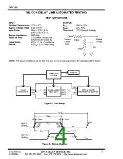
3D7323
APPLICATION NOTES (CONT’D)
circuitry to minimize the delay variations induced
by fluctuations in power supply and/or
temperature.
custom reference designator identifying the
intended frequency and duty cycle of operation.
The programmed delay accuracy of the device is
guaranteed, therefore, only for the user specified
input characteristics. Small input pulse width
variation about the selected pulse width will only
marginally impact the programmed delay
The thermal coefficient is reduced to 300
PPM/C, which is equivalent to a variation , over
the -40C to 85C operating range, of ±3% from
the room-temperature delay settings and/or
1.0ns, whichever is greater. The power supply
coefficient is reduced, over the 4.75V to 5.25V
operating range, to ±1% of the delay settings at
the nominal 5.0VDC power supply and/or 2.0ns,
whichever is greater. It is essential that the
power supply pin be adequately bypassed
and filtered. In addition, the power bus
should be of as low an impedance
accuracy, if at all. Nevertheless, it is strongly
recommended that the engineering staff at
DATA DELAY DEVICES be consulted.
POWER SUPPLY AND
TEMPERATURE CONSIDERATIONS
The delay of CMOS integrated circuits is strongly
dependent on power supply and temperature.
The monolithic 3D7323 programmable delay line
utilizes novel and innovative compensation
construction as possible. Power planes are
preferred.
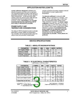
DEVICE SPECIFICATIONS
TABLE 2: ABSOLUTE MAXIMUM RATINGS
PARAMETER
DC Supply Voltage
Input Pin Voltage
Input Pin Current
Storage Temperature
Lead Temperature
SYMBOL
VDD
MIN
-0.3
-0.3
-1.0
-55
MAX
7.0
UNITS NOTES
V
V
VIN
VDD+0.3
1.0
IIN
TSTRG
TLEAD
mA
C
25C
150
300
C
10 sec
TABLE 3: DC ELECTRICAL CHARACTERISTICS
(-40C to 85C, 4.75V to 5.25V)
PARAMETER
SYMBOL
MIN
MAX
UNITS
mA
V
NOTES
Static Supply Current*
High Level Input Voltage
Low Level Input Voltage
High Level Input Current
Low Level Input Current
High Level Output Current
IDD
VIH
VIL
IIH
5
2.0
0.8
1
V
-1
-1
VIH = VDD
VIL = 0V
VDD = 4.75V
VOH = 2.4V
VDD = 4.75V
VOL = 0.4V
CLD = 5 pf
µA
IIL
IOH
1
µA
-4.0
mA
Low Level Output Current
IOL
4.0
mA
ns
Output Rise & Fall Time
TR & TF
2
*IDD(Dynamic) = 3 * CLD * VDD * F
Input Capacitance = 10 pf typical
Output Load Capacitance (CLD) = 25 pf max
where: CLD = Average capacitance load/line (pf)
F = Input frequency (GHz)
Doc #06015
5/10/2006
DATA DELAY DEVICES, INC.
3
3 Mt. Prospect Ave. Clifton, NJ 07013

 DATADELAY [ DATA DELAY DEVICES, INC. ]