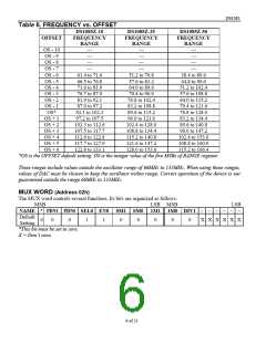
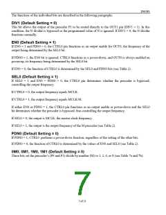
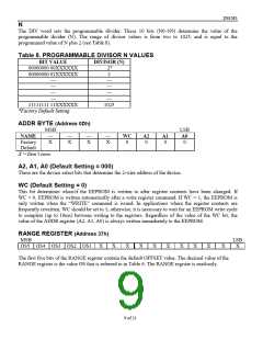
DS1085
COMMAND SET
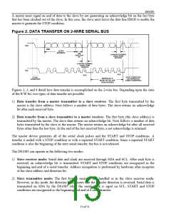
Data and control information is read from and written to the DS1085 in the format shown in Figure 3. To
write to the DS1085, the master issues the slave address of the DS1085 and the R/ W bit is set to 0. After
receiving an acknowledge, the bus master provides a command protocol. After receiving this protocol, the
DS1085 issues an acknowledge, and then the master can send data to the DS1085. If the DS1085 is to be
read, the master must send the command protocol as before, and then issue a repeat START condition and
then the control byte again, this time with the R/ W bit set to 1 to allow reading of the data from the
DS1085. The command set for the DS1085 is as follows:
Access DAC [08h]
If R/ W is 0, this command writes to the DAC register. After issuing this command, the next data byte
values are written into the DAC register. If R/ W is 1, the next data bytes read are the values stored in the
DAC register. This is a 2-byte transfer, the first byte contains the eight MSBs, the second byte contains
the two LSBs in the most significant positions of the data byte. The remaining six bits are ignored and
can be written with any value (if read, these bits are 0).
Access OFFSET [0Eh]
If R/ W is 0, this command writes to the OFFSET register. After issuing this command, the next data byte
value is written into the OFFSET register. If R/ W is 1, the next data byte read is the value stored in the
OFFSET register. This is a single byte transfer of which only the five LSBs (last five bits) are used. The
remaining three bits can be written with any value to complete the data byte (if read, these bits are 1).
Access DIV [01h]
If R/ W is 0, this command writes to the DIV register. After issuing this command, the next data byte
values are written into the DIV register. If R/ W is 1, the next data bytes read are the values stored in the
DIV register. This register has a 10-bit value. The upper eight bits are sent first, followed by a second
byte that contains the two LSBs of the register value in the most significant positions of the data byte.
The remaining six bits are ignored and can be set to any value (if read, these bits are 0).
Access MUX [02h]
If R/ W is 0, this command writes to the MUX register. After issuing this command, the next data byte
values are written into the MUX register. If R/ W is 1, the next data bytes read are the values stored in the
MUX register. This register has a 10-bit value. The upper eight bits are sent first, followed by a second
byte that contains the two LSBs of the register value in the most significant positions of the data byte.
The remaining six bits are ignored and can be set to any value (if read, these bits are 0).
Access ADDR [0Dh]
If R/ W is 0, this command writes to the ADDR register. After issuing this command, the next data byte
value is written into the ADDR register. If R/ W is 1, the next data byte read is the value stored in the
ADDR register. This is a single-byte transfer. This register has a 5-bit value, the first three bits of a write
can be any value followed by the five active bits (if read, the first three bits are 0).
10 of 21

 DALLAS [ DALLAS SEMICONDUCTOR ]