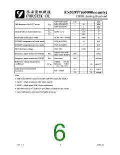
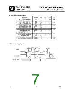
ES51997(60000counts)
DMM Analog front end
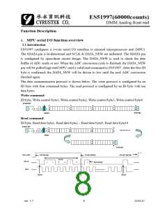
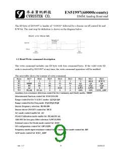
The read command includes one ID byte with ten data bytes. When DATA_NEW is ready1,
MPU could send the read data command to get the result of ADC conversion
(D0/D1/D2/D3)2 or status flag from ES51997.
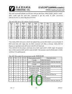
The next table shows the content of read command.
Byte
ID
R1
R2
R3
R4
R5
R6
R7
Bit7
1
ASIGN
HF
D0:3
D0:11
D1:0
D1:8
D2:6
D2:14
D3:3
D3:11
Bit6
1
BSIGN
LF
D0:4
D0:12
D1:1
D1:9
D2:7
D2:15
D3:4
D3:12
Bit5
0
PMAX
LDUTY
D0:5
D0:13
D1:2
D2:0
Bit4
0
Bit3
1
Bit2
0
Bit1
BUZ
STA0
D0:1
D0:9
D0:17
D1:6
D2:4
D2:12
D3:1
D3:9
D3:17
Bit0
R/W=1
ALARM
D0:2
D0:10
D0:18
D1:7
D2:5
D2:13
D3:2
PMIN
STA1
D0:6
D0:14
D1:3
D2:1
D2:9
D2:17
D3:6
D3:14
BTS0
F_FIN
D0:7
D0:15
D1:4
D2:2
D2:10
D2:18
D3:7
D3:15
BTS1
D0:0
D0:8
D0:16
D1:5
D2:3
D2:11
D3:0
D3:8
D3:16
D2:8
D2:16
D3:5
R8
R9
R10
D3:10
D3:18
D3:13
1Note: DATA_NEW will be active with D1 data updated when one fast ADC (FADC) conversion finished. If
MCU access slow ADC output only, ten FADC conversion cycle delay is necessary. DATA_NEW for
frequency or capacitance mode will be active when D0 or D3 data ready.
2Note: D0/D1/D2/D3 all are binary code format. D0 is SADC output and D1 is FADC output. The maximum
data is 63000 counts for SADC and 604 counts for FADC. The maximum counts for PEAK mode is 103000,
so D0 bit 17-18 could be ignored..
The ADC data output for measurement mode: F3/F2/F1/F0
F3
0
0
0
0
0
0
0
0
1
1
1
F2
0
0
0
0
1
1
1
1
0
0
0
F1
0
0
1
1
0
0
1
1
0
0
1
F0
0
1
0
1
0
1
0
1
0
1
0
Measurement mode
V mode
Read data bytes
D0(0:18), D1(0:9)
D0(0:18), D1(0:9), D2(0:18), D3(0:18)
D0(0:18), D1(0:9)
ACV + Hz(%) mode
A mode
D0(0:18), D1(0:9), D2(0:18), D3(0:18)
D0(0:18), D1(0:9)
ACA + Hz(%) mode
Resistance mode
Continuity mode
Diode mode
D0(0:18), D1(0:9)
D0(0:18), D1(0:9)
D0(0:18), D2(0:18), D3(0:18)
D0(0:18)
F + duty mode
Capacitance Mode
ADP mode
D0(0:18), D1(0:9)
D0(0:18), D1(0:9), D2(0:18), D3(0:18)
ADP + Hz(%) mode
ver. 1.7
10
12/01/12

 CYRUSTEK [ Cyrustek corporation ]