CY7C68300B/CY7C68301B
CY7C68320/CY7C68321
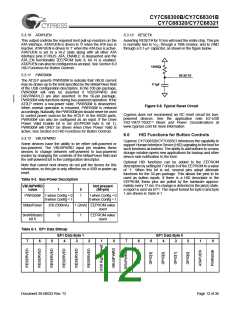
5.3.10 ATAPUEN
5.3.13 RESET#
This output controls the required host pull-up resistors on the
ATA interface. ATAPUEN is driven to ‘0’ when the ATA bus is
inactive. ATAPUEN is driven to ‘1’ when the ATA bus is active.
ATAPUEN is set to a Hi-Z state along with all other ATA
interface pins if VBUS_ATA_ENABLE is deasserted and the
ATA_EN functionality (EEPROM byte 8, bit 4) is enabled.
ATAPUEN can also be configured as an input. See Section 6.0
HID Functions for Button Controls
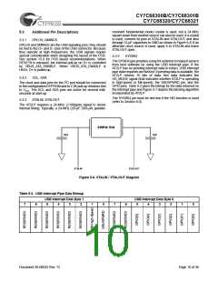
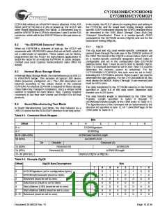
Asserting RESET# for 10 ms will reset the entire chip. This pin
is normally tied to VCC through a 100k resistor, and to GND
through a 0.1-µF capacitor, as shown in the figure below.
100KΩ
RESET#
0.1µF
5.3.11 PWR500#
The AT2LP asserts PWR500# to indicate that VBUS current
may be drawn up to the limit specified by the bMaxPower field
of the USB configuration descriptors. In the 100-pin package,
PWR500# will only be asserted if VBUSPWRD and
DRVPWRVLD are also asserted. In the 56-pin package,
PWR500# only functions during bus-powered operation. If the
AT2LP enters a low-power state, PWR500# is deasserted.
When normal operation is resumed, PWR500# is restored
accordingly. Naturally, the PWR500# pin should never be used
to control power sources for the AT2LP. In the 68320 parts,
PWR500# can also be configured as an input. If the Drive
Power Valid Enable bit is set (EEPROM byte 8, bit 1),
PWR500# will ONLY be driven when Drive Power Valid is
active. See Section 6.0 HID Functions for Button Controls.
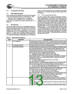
Figure 5-8. Typical Reset Circuit
Cypress does not recommend an RC reset circuit for bus-
powered devices. See the application note EZ-USB
FX2 /AT2 /SX2
Reset and Power Considerations at
www.cypress.com for more information.
6.0
HID Functions for Button Controls
5.3.12 VBUSPWRD
Cypress’ CY7C68320/CY7C68321 introduces the capability to
support Human Interface Device (HID) signaling to the host for
such functions as buttons. The ability to add buttons to a mass
storage solution opens new applications for backup and other
device-side notification to the host.
Some devices have the ability to be either self-powered or
bus-powered. The VBUSPWRD input pin enables these
devices to change between self-powered to bus-powered
modes by changing the contents of the bMaxPower field and
the self-powered bit in the configuration descriptor.
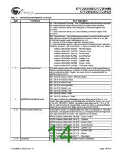
Optional HID functions can be added to the EEPROM
descriptors by setting bit 7 of byte 8 of the EEPROM to a value
of ‘1’. When this bit is set, several pins adopt alternate
functions for the 56-pin package. This allows the pins to be
used as button inputs. If there is a HID descriptor in the
EEPROM, these pins are polled by the hardware approxi-
mately every 17 ms. If a change is detected in the pin(s) state,
a report is sent via EP1. The report format for byte 0 and byte
1 are shown in Table 6-1.
Note that current host drivers do not poll the device for this
information, so this pin is only effective on a USB or power-up
reset.
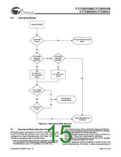
Table 5-3. Bus-Power Description
VBUSPWRD
value
Not present
(56-pin)
1
0
PWR500# 1 when Config = 0
0 when Config = 1
1
1 when Config = 0
0 when Config = 1
bMaxPower
250 (500mA)
1 (2mA) EEPROM value
used
bmAttributes
bit 6
0
1
EEPROM value
used
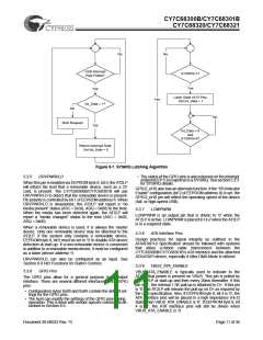
Table 6-1. EP1 Data Bitmap
EP1 Data Byte 1
EP1 Data Byte 0
7
6
5
4
3
2
1
0
7
6
5
4
3
2
1
0
Document 38-08033 Rev. *D
Page 12 of 36

 CYPRESS [ CYPRESS ]