CY7C68013A/CY7C68014A
CY7C68015A/CY7C68016A
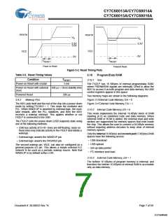
RESET#
RESET#
VIL
VIL
3.3V
3.0V
3.3V
VCC
VCC
0V
0V
TRESET
TRESET
Power on Reset
Powered Reset
Figure 3-2. Reset Timing Plots
Table 3-5. Reset Timing Values
3.10
Program/Data RAM
Condition
TRESET
3.10.1 Size
Power-on Reset with crystal
5 ms
The FX2LP has 16 KBytes of internal program/data RAM,
where PSEN#/RD# signals are internally ORed to allow the
8051 to access it as both program and data memory. No USB
control registers appear in this space.
Power-on Reset with external 200 µs + Clock stability time
clock
Powered Reset
200 µs
Two memory maps are shown in the following diagrams:
Figure 3-3 Internal Code Memory, EA = 0
3.9.2 Wakeup Pins
The 8051 puts itself and the rest of the chip into a power-down
mode by setting PCON.0 = 1. This stops the oscillator and
PLL. When WAKEUP is asserted by external logic, the oscil-
lator restarts, after the PLL stabilizes, and then the 8051
receives a wakeup interrupt. This applies whether or not
FX2LP is connected to the USB.
Figure 3-4 External Code Memory, EA = 1.
3.10.2 Internal Code Memory, EA = 0
This mode implements the internal 16-KByte block of RAM
(starting at 0) as combined code and data memory. When
external RAM or ROM is added, the external read and write
strobes are suppressed for memory spaces that exist inside
the chip. This allows the user to connect a 64-KByte memory
without requiring address decodes to keep clear of internal
memory spaces.
The FX2LP exits the power-down (USB suspend) state using
one of the following methods:
• USB bus activity (if D+/D– lines are left floating, noise on
these lines may indicate activity to the FX2LP and initiate a
wakeup).
Only the internal 16 KBytes and scratch pad 0.5 KBytes RAM
spaces have the following access:
• External logic asserts the WAKEUP pin
• External logic asserts the PA3/WU2 pin.
• USB download
• USB upload
The second wakeup pin, WU2, can also be configured as a
general purpose I/O pin. This allows a simple external R-C
network to be used as a periodic wakeup source. Note that
WAKEUP is by default active LOW.
• Set-up data pointer
• I2C interface boot load.
3.10.3 External Code Memory, EA = 1
The bottom 16 KBytes of program memory is external, and
therefore the bottom 16 KBytes of internal RAM is accessible
only as data memory.
Document #: 38-08032 Rev. *K
Page 7 of 60
[+] Feedback

 CYPRESS [ CYPRESS ]