FOR
FOR
CY7C63411/12/13
CY7C63511/12/13
CY7C63612/13
7.0
Clocking
Clock Distribution
XTALOUT
XTALIN
clk1x
(to USB SIE)
Clock
Doubler
clk2x
(to Microcontroller)
30 pF
30 pF
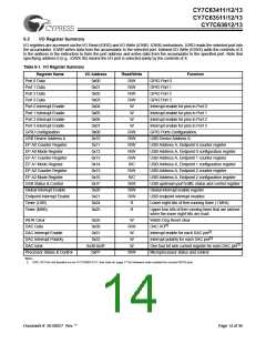
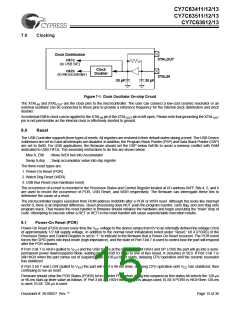
Figure 7-1. Clock Oscillator On-chip Circuit
The XTALIN and XTALOUT are the clock pins to the microcontroller. The user can connect a low-cost ceramic resonator or an
external oscillator can be connected to these pins to provide a reference frequency for the internal clock distribution and clock
doubler.
An external 6 MHz clock can be applied to the XTALIN pin if the XTALOUT pin is left open. Please note that grounding the XTALOUT
pin is not permissible as the internal clock is effectively shorted to ground.
8.0
Reset
The USB Controller supports three types of resets. All registers are restored to their default states during a reset. The USB Device
Addresses are set to 0 and all interrupts are disabled. In addition, the Program Stack Pointer (PSP) and Data Stack Pointer (DSP)
are set to 0x00. For USB applications, the firmware should set the DSP below 0xE8h to avoid a memory conflict with RAM
dedicated to USB FIFOs. The assembly instructions to do this are shown below:
Mov A, E8h
; Move 0xE8 hex into Accumulator
Swap A,dsp ; Swap accumulator value into dsp register
The three reset types are:
1. Power-On Reset (POR)
2. Watch Dog Reset (WDR)
3. USB Bus Reset (non hardware reset)
The occurrence of a reset is recorded in the Processor Status and Control Register located at I/O address 0xFF. Bits 4, 5, and 6
are used to record the occurrence of POR, USB Reset, and WDR respectively. The firmware can interrogate these bits to
determine the cause of a reset.
The microcontroller begins execution from ROM address 0x0000h after a POR or WDR reset. Although this looks like interrupt
vector 0, there is an important difference. Reset processing does NOT push the program counter, carry flag, and zero flag onto
program stack. That means the reset handler in firmware should initialize the hardware and begin executing the “main” loop of
code. Attempting to execute either a RET or RETI in the reset handler will cause unpredictable execution results.
8.1
Power-On Reset (POR)
Power-On Reset (POR) occurs every time the VCC voltage to the device ramps from 0V to an internally defined trip voltage (Vrst)
of approximately 1/2 full supply voltage. In addition to the normal reset initialization noted under “Reset,” bit 4 (PORS) of the
Processor Status and Control Register is set to “1” to indicate to the firmware that a Power-On Reset occurred. The POR event
forces the GPIO ports into input mode (high impedance), and the state of Port 3 bit 7 is used to control how the part will respond
after the POR releases.
If Port 3 bit 7 is HIGH (pulled to VCC) and the USB IO are at the idle state (DM HIGH and DP LOW) the part will go into a semi-
permanent power down/suspend mode, waiting for the USB IO to go to one of Bus Reset, K (resume) or SE0. If Port 3 bit 7 is
still HIGH when the part comes out of suspend, then a 128-µs timer starts, delaying CPU operation until the ceramic resonator
has stabilized.
If Port 3 bit 7 was LOW (pulled to VSS) the part will start a 96-ms timer, delaying CPU operation until VCC has stabilized, then
continuing to run as reset.
Firmware should clear the POR Status (PORS) bit in register FFh before going into suspend as this status bit selects the 128-µs
or 96-ms start-up timer value as follows: IF Port 3 bit 7 is HIGH then 128-µs is always used; ELSE if PORS is HIGH then 128-ms
is used; ELSE 128-µs is used.
Document #: 38-08027 Rev. **
Page 15 of 36

 CYPRESS [ CYPRESS ]