B.1.1 Memory Organization
Memory organization in the 8051 core is similar to that of the industry standard 8051. There
are three distinct memory areas: program memory (ROM), data memory (external RAM), and
registers (internal RAM).
B.1.1.1 Program Memory
The EZ-USB provides 8K of data that is mapped as both program and data memory at
addresses 0x0000-0x1B3F. In addition, the bulk endpoint buffers may be used as external data
memory if they are not used as endpoint buffers. See Chapter 3, "EZ-USB Memory" for more
details.
B.1.1.2 External RAM
The EZ-USB chip has dedicated address and data pins, so port 2 and port 0 are not used to
access the memory bus. As shown in Chapter 3, "EZ-USB Memory", the EZ-USB is
expandable to over 100K of external program and data memory.
B.1.1.3 Internal RAM
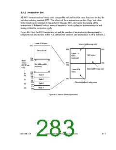
The internal RAM (Figure B-2) consists of:
•
•
•
128 bytes of registers and scratch pad memory accessible through direct or indirect
addressing (addresses 00h–7Fh).
A 128 register space for special function registers (SFRs) accessible through direct
addressing (addresses 80h–FFh).
Upper 128 bytes of scratch pad memory accessible through indirect addressing
(addresses 80h–FFh).
Although the SFR space and the upper 128 bytes of RAM share the same address range, the
actual address space is separate and is differentiated by the type of addressing. Direct
addressing accesses the SFRs, and indirect addressing accesses the upper 128 bytes of RAM.
The lower 128 bytes are organized as shown in Figure B-2. The lower 32 bytes (0x00-0xIF)
form four banks of eight registers (R0–R7). Two bits on the program status word (PSW) select
which bank is in use. The next 16 bytes (0x20 - 0x2F) form a block of bit-addressable memory
space at bit addresses 0h-7Fh. All of the bytes in the lower 128 bytes are accessible through
direct or indirect addressing.
The SFRs occupy addresses 80h–FFh and are only accessible through direct addressing. Most
SFRs are reserved for specific functions as described in the “Special Function Registers” on
page B-12.
SFR addresses ending in 0h or 8h are bit-addressable.
B - 2
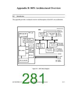
Appendix B: 8051 Architectural Overview
EZ-USB TRM v1.9

 CYPRESS [ CYPRESS ]