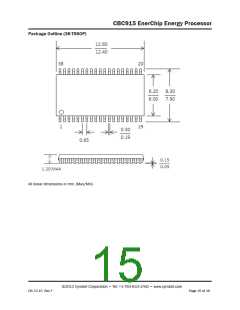
CBC915 EnerChip Energy Processor
Important EnerChip EP Pin Connections
The DVDD and AVDD pins should be connected together on the printed circuit board.
The DVSS and AVSS pins should be connected together on the printed circuit board.
The DVDD pin should be connected with bypass cap to the DVSS pin - typical capacitance value is 0.1uF; place
as close to pins 2 and 4 as possible and in parallel a 10uF cap for low frequency decoupling
The AVDD pin should be connected with bypass cap to the AVSS pin - typical capacitance value is 0.1uF; place
as close to pins 2 and 4 as possible and in parallel with a 10uF cap for low frequency decoupling.
Remember the Status Indicators: EC CHG/ (EnerChip Charge) te, CAP CHG/ (Capacitor Charge) and MPPT/
(Maximum Peak Power Tracking) must be connected to a reistor pull up or LED to insure the CBC915 has a
method of shedding excess harvested energy.
Printed Circuit Board (PCB) Layout Guidelines for the CBC915 Application Circuit
The boost converter power stage consists of elements with tens of milliamperes of current along with control
electronics with very high impedances operating at only a few nanoamperes of current. This disparity between
current densities in the power stage vs. the control circuits can lead to poor circuit performance, poor efficiency
and excessive noise coupling into other circuits if careful layout practices are not observed.
As in most switch mode power supply layouts, it is usually advantageous to isolate the power stage from the
control electronics through a combination of isolated current conductors or by careful placement of power stage
components in such a manner that the high currents in the power stage stay in an area associated only with
the power stage components. Proper design and layout of the CBC915 application circuit will ensure maximum
circuit performance.
Power stage components Cin, L, Q, D1, D2, and Cout should all be in close physical proximity to each other.
When placing the components, it is better to make the traces associated with Cout the shorter path. The signal
return conduction path should either be at the edge or corner of the board if a common ground plane is used,
or routed together outside of the ground plane and then tied to the ground plane at a single point - preferably
at the signal return connection for Cout. All traces interconnecting the power components should be as short
and wide as practical; this will help eliminate parasitic inductance and conducted losses which will in turn
help keep conducted noise and magnetic fields out of adjacent circuits. Doing a good job with the power stage
component placement and layout will yield the best performance of the system as a whole. This area should not
be compromised if maximum performance is to be achieved.
The feedback resistors R1 and R2 should be as close as practical to the VGSENSE input on the CBC915. The
signal return line for resistor R2 should be isolated from the high current power stage signal return lines, either
by placement of the components relative to the power stage components or by providing separate return lines.
Place bypass capacitors as near to the CBC915 VDD and VSS pins as possible. If using a power and ground
plane, drop vias directly from the bypass capacitors to the power and ground planes and from the CBC915 VDD
and VSS pins directly to the power and ground planes.
In general, all discrete components should be placed physically close to the gate connection of the transistor they
are associated with. Keep the node lengths as short as possible to the FET gate connections.
Follow the PCB layout guidelines in the EnerChip data sheet and User Manual for details on how to minimize stray
leakage paths on EnerChip package pins and PCB routing traces.
©2012 Cymbet Corporation • Tel: +1-763-633-1780 • www.cymbet.com
DS-72-15 Rev F
Page 14 of 16

 CYMBET [ CYMBET CORPORATION ]