Additional Resources: Product Page
|
3D Model
|
PCB Footprint
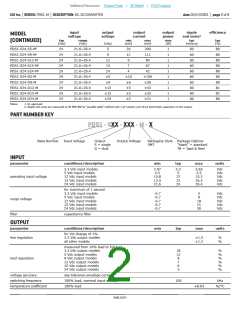
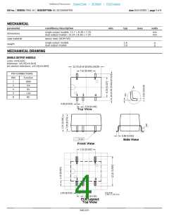
CUI Inc │ SERIES: PDS1-M │ DESCRIPTION: DC-DC CONVERTER
date 03/14/2021 │ page 7 of 8
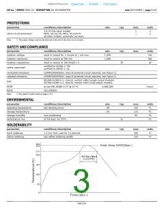
APPLICATION NOTES
1. Output load requirement
To ensure this module can operate efficiently and reliably, the minimum output load may not be less than 10% of the full load during
operation. If the actual output power is low, connect a resistor at the output end in parallel to increase the load.
2. Overload Protection
Under normal operating conditions, the output circuit of this product has no protection against overload. The simplest method to add
this is to add a circuit breaker to the circuit.
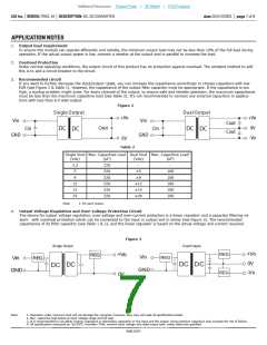
3. Recommended circuit
If you want to further decrease the input/output ripple, you can increase the capacitance accordingly or choose capacitors with low
ESR (see Figure 2 & Table 1). However, the capacitance of the output filter capacitor must be appropriate. If the capacitance is too
high, a startup problem might arise. For every channel of the output, to ensure safe and reliable operation, the maximum capacitance
must be less than the maximum capacitive load (see Table 2). It’s not recommended to connect any external capacitors in applica-
tions with less than 0.5 watt output.
Figure 2
Single Output
Dual Output
+Vo
+Vo
0V
Vin
Vin
Cout
Cout
Cout
Cin
Cin
DC
DC
DC
DC
GND
GND
-Vo
0V
Table 2
Max. Capacitive Load1
Single Vout Max. Capacitive Load Dual Vout
(μF)
(Vdc)
3.3
5
(μF)
220
220
220
220
220
220
(Vdc)
-
-
±5
100
100
100
100
100
9
±9
12
15
24
±12
±15
±24
Note:
1. For each output.
4. Output Voltage Regulation and Over-voltage Protection Circuit
The device for output voltage regulation, over-voltage and over-current protection is a linear regulator and a capacitor filtering ne
work with overheat protection which can be connected to the input or output end in series (see Figure 3). The recommended
capacitance of its filter capacitor (see Table 1 & 2), and the linear regulator is based on the actual voltage and current required.
Figure 3
Single Output
Dual Output
+Vo
0V
REG
REG
+Vo
0V
REG
Vin
REG
Vin
REG
DC DC
DC
DC
GND
GND
-Vo
Note:
1. Operation under minimum load will not damage the converter; however, they may not meet all specifications listed.
2. Max. capacitive load tested at input voltage range and full load.
3. It is recommended to use either ceramic capacitors or electrolytic capacitors on the input and the output. Using tantalum capacitors may increase the risk of failure.
4. All specifications measured at: Ta=25°C, humidity<75%, nominal input voltage and rated output load, unless otherwise specified.
cui.com

 CUI [ CUI INC ]