CBM8521-CBM8522-CBM8523-CBM8524
OPERATION INSTRUCTION
APPLICATION NOTES
The CBM8521, CBM8522, CBM8523, CBM8524
series op amps are unity-gain stable and free from
unexpected output phase reversal. They use
auto-zeroing techniques to provide low offset voltage
and very low drift over time and temperature.
signal can be up to 5.5V above the negative supply,
independent of the positive supply voltage. A valid
logic low is defined as < 0.8V above the V– supply pin.
If dual or split power supplies are used, be sure that
logic input signals are properly referred to the
negative supply voltage. The Enable pin must be
connected to a valid high or low voltage, or driven,
not left open circuit.
Good layout practice mandates use of a 0.1μF
capacitor placed closely across the supply pins.
For lowest offset voltage and precision
performance,
circuit
layout
and
mechanical
The logic input is a high-impedance CMOS input,
with separate logic inputs provided on the dual
version. For battery operated applications, this
feature can be used to greatly reduce the average
current and extend battery life.
conditions should be optimized. Avoid temperature
gradients that create thermoelectric (Seebeck) effects
in thermocouple junctions formed from connecting
dissimilar conductors. These thermally-generated
potentials can be made to cancel by assuring that
they are equal on both input terminals.
The enable time includes one full auto zero cycle
required by the amplifier to return to VOS accuracy.
Prior to this time, the amplifier functions properly, but
with unspecified offset voltage.
Use low thermoelectric-coefficient connections
(avoid dissimilar metals).
Thermally isolate components from power
supplies or other heat-sources.
Disable time is 1μs. When disabled, the output
assumes a high-impedance state. This allows the
CBM8523 to be operated as a gated amplifier, or to
have the output multiplexed onto a common analog
output bus.
Shield op amp and input circuitry from air
currents, such as cooling fans.
Following these guidelines will reduce the
likelihood
of
junctions
being
at
different
temperatures, which can cause thermoelectric
voltages of 0.1μV/°C or higher, depending on
materials used.
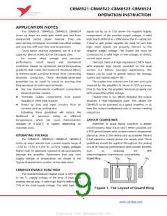
LAYOUT GUIDELINES
Attention to good layout practices is always
recommended. Keep traces short. When possible, use
a PCB ground plane with surface-mount components
placed as close to the device pins as possible. Place a
0.1μF capacitor closely across the supply pins. These
guidelines should be applied throughout the analog
circuit to improve performance and provide benefits
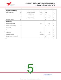
OPERATING VOLTAGE
The CBM8521, CBM8522, CBM8523, CBM8524
series op amps operate over a power-supply range of
+2.5V to +5.5V (±1.25V to ±2.75V). Supply voltages
higher than 7V (absolute maximum) can permanently
damage the amplifier. Parameters that vary over
supply voltage or temperature are shown in the
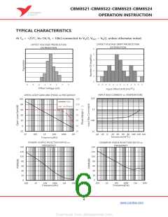
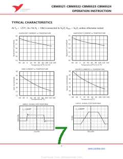
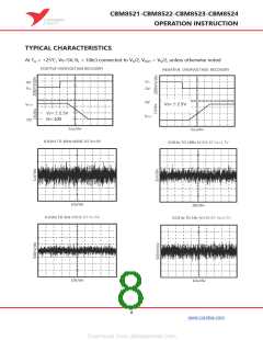
Typical Characteristics section of this data sheet.
such
as
reducing
the
EMI
(electromagnetic-interference) susceptibility
CBM8523 ENABLE FUNCTION
The enable/shutdown digital input is referenced
to the V– supply voltage of the amp. A logic high
enables the op amp. A valid logic high is defined as >
75% of the total supply voltage. The valid logic high
9
www.corebai.com

 COREBAI [ Corebai ]