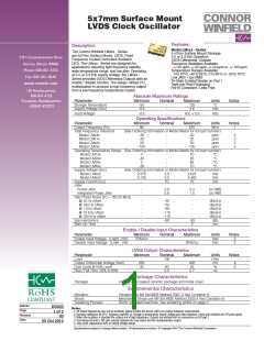
2111 Comprehensive Drive
Aurora, Illinois 60505
Phone: 630-851-4722
Fax: 630-851-5040
www.conwin.com
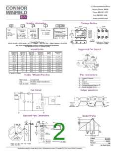
Ordering Information
Package Outline
LM
1
2
3
- 155.52M
0.275
(7.0mm)
0.055
(1.4mm)
Output Frequency
Type
LVDS
Temperature
Range
Frequency
Tolerance
Supply Voltage
Frequency Format
-xxx.xM Min
-xxx.xxxxxxM Max
*Amount of numbers
after the decimal
point. M = MHz
CW
1040
LM123
155.52 MHZ
2 = 2.5 Vdc,
3 = 3.3 Vdc,
0.197
(5.0mm)
Clock Series 1 = 0 to 70°C
4 = 20 ppm
1 = 25 ppm
2 = 50 ppm
3 = 100 ppm
5x7 mm
2 = -40 to 85°C
3 = 0 to 85°C
4 = -20 to 70°C
0.102
(2.6mm)
.069
(1.75mm)
Example Part Number:
Dimensional Tolerance
+/-0.008 (+/-0.2mm)
LM123-155.52M = LVDS Output, 0 to 70°C, +/-50ppm, 3.3Vdc, E/D Pad 1, Output Frequency 155.52 MHz
Note: Not all temperature and frequency tolerance combinations are available.
See Model Matrix below for available models
Model Matrix
Suggested Pad Layout
Frequency
Tolerance
±±2 ppm
Frequency
Tolerance
±±ꢀ ppm
Frequency
Tolerance
±ꢀ2 ppm
Frequency
Tolerance
±ꢁ22 ppm
Supply
Voltage
Temperature
Range
0.200
(5.08mm)
0.100
LM142
LM442
LM342
X
LM112
LM412
LM312
X
LM122
LM422
LM322
LM222
LM123
LM423
LM323
LM223
LM132
LM432
LM332
LM232
LM133
LM433
LM333
LM233
2.5 Vdc
2.5 Vdc
2.5 Vdc
2.5 Vdc
3.3 Vdc
3.3 Vdc
3.3 Vdc
3.3 Vdc
0 to 70°C
-20 to 70°C
0 to 85°C
(2.54mm)
6
5
4
3
0.079
(2.0mm)
Top
View
0.165
(4.2mm)
-40 to 85°C
0 to 70°C
Bypass
Capacitor
0.01uF
LM143
LM443
LM343
X
LM113
LM413
LM313
X
1
2
-20 to 70°C
0 to 85°C
Ground
0.070
(1.78mm)
-40 to 85°C
X = Models not available
Enable / Disable Function
Pad Connections
1: Enable / Disable
Pad 1 Input:
Low:
High or Open: Enabled
Output State:
2
N/C
Disabled (High Impedance)
3: Ground
4: Output Q
5: Complementary Output Q
6: Supply Voltage (Vcc)
Test Circuit
Output Waveform
Vcc
Power
Supply
Duty Cycle
Q
Q
Q
Vod
Vod
Ground
100
Ohm
0.01 uF
Differential
Output
80%
20%
Vopp
0V
0V
0V
Q
Waveform
peak-to-peak
tf
E/D
tr
N/C
Tape and Reel Dimensions
Solder Profile
260°C
Temperature
260°C
220°C
180°C
150°C
120°C
0
Time
120 S
10 S
Max.
60 S
Max.
360 Sec. Max.
Bulletin
Page
Ds030
2 of 2
00
Dimensional Tolerance: ± ±.02 ꢀ±ꢁ.ꢂmmꢃ
± ±..ꢁ2 ꢀ±ꢄ0ꢅmmꢃ
Revision
Date
05 Oct 2010
Specifications subject to change without notice. All dimensions in inches. © Copyright 2010 The Connor-Winfield Corporation

 CONNOR-WINFIELD [ CONNOR-WINFIELD CORPORATION ]