PDF
最近搜索
热门搜索
发布采购

| 型号: | RS8953BEPJ |
| PDF下载: | 下载PDF文件 查看货源 |
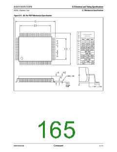
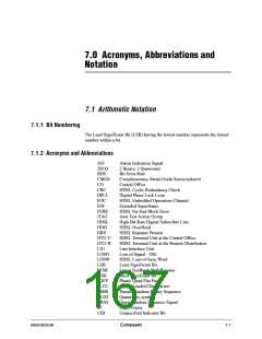
| 内容描述: | 高比特率数字用户线( HDSL )信道单元 [High-Bit-Rate Digital Subscriber Line (HDSL) channel unit] |
| 分类和应用: | 电信集成电路 |
| 文件页数/大小: | 173 页 / 1229 K |
| 品牌: |  CONEXANT [ CONEXANT SYSTEMS, INC ] CONEXANT [ CONEXANT SYSTEMS, INC ] |
专业IC领域供求交易平台:提供全面的IC Datasheet资料和资讯,Datasheet 1000万数据,IC品牌1000多家。