CX11656 HomePlug 1.0 PHY Data Sheet
Contents
1. Introduction......................................................................................................................................... 1-1
1.1
1.2
1.3
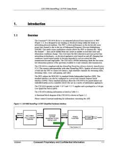
Overview .....................................................................................................................................................................1-1
Features ......................................................................................................................................................................1-3
Applications ................................................................................................................................................................1-3
2. Hardware Interface .............................................................................................................................. 2-1
2.1
2.2
CX11656 PHY Hardware Interface Signals...................................................................................................................2-1
CX11656 PHY Electrical and Environmental Specifications..........................................................................................2-9
3. CX11656 Functional Description.......................................................................................................... 3-1
3.1
MII Data Interface with MDI Control ............................................................................................................................3-2
3.1.1
MII Interface................................................................................................................................................3-3
3.1.1.1
3.1.1.2
3.1.1.3
MII Timing Diagram.................................................................................................................3-3
MII Signal Descriptions............................................................................................................3-6
MII Frame Structure.................................................................................................................3-8
3.1.2
3.1.3
MDI Control Interface ..................................................................................................................................3-9
3.1.2.1 MDI Signal Descriptions ........................................................................................................3-10
MII Management Register Set ...................................................................................................................3-10
3.1.3.1
3.1.3.2
3.1.3.3
3.1.3.4
3.1.3.5
3.1.3.6
3.1.3.7
PRE (Preamble) .....................................................................................................................3-10
ST (Start of Frame) ................................................................................................................3-10
OP (Operation Code)..............................................................................................................3-11
PHYAD (PHY Address)...........................................................................................................3-11
REGAD (Register Address).....................................................................................................3-11
TA (Turnaround) ....................................................................................................................3-11
Data.......................................................................................................................................3-11
3.2
GPSI Interface with SPI Control.................................................................................................................................3-12
3.2.1
GSPI Interface ...........................................................................................................................................3-12
3.2.1.1
3.2.1.2
3.2.1.3
GPSI Timing Diagrams...........................................................................................................3-12
GPSI DC Characteristics.........................................................................................................3-14
GPSI Signal Descriptions.......................................................................................................3-14
3.2.2
SPI Slave Port Interface.............................................................................................................................3-15
3.2.2.1
3.2.2.2
SPI Slave Port Signal Timing .................................................................................................3-15
SPI Slave Port DC Characteristics ..........................................................................................3-16
102069A
Conexant Proprietary and Confidential Information
iii

 CONEXANT [ CONEXANT SYSTEMS, INC ]