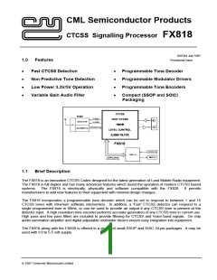
CTCSS Signalling Processor
FX818
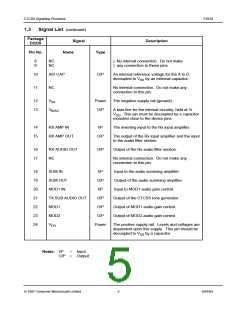
1.3
Signal List (continued)
Package
D2/D5
Signal
Name
Description
Pin No.
Type
8
9
NC
NC
) No internal connection. Do not make
) any connection to these pins.
10
11
A/D CAP
NC
O/P
An internal reference voltage for the A to D,
decoupled to V by an external capacitor.
SS
No internal connection. Do not make any
connection to this pin.
12
13
V
V
Power
O/P
The negative supply rail (ground).
ss
A bias line for the internal circuitry, held at ½
BIAS
V . This pin must be decoupled by a capacitor
DD
mounted close to the device pins.
14
15
RX AMP IN
I/P
The inverting input to the Rx input amplifier.
RX AMP OUT
O/P
The output of the Rx input amplifier and the input
to the audio filter section.
16
17
RX AUDIO OUT
NC
O/P
Output of the Rx audio filter section.
No internal connection. Do not make any
connection to this pin.
18
19
20
21
22
23
24
SUM IN
I/P
O/P
I/P
Input to the audio summing amplifier.
Output of the audio summing amplifier.
Input to MOD1 audio gain control.
Output of the CTCSS tone generator.
Output of MOD1 audio gain control.
Output of MOD2 audio gain control.
SUM OUT
MOD1 IN
TX SUB AUDIO OUT
MOD1
O/P
O/P
O/P
Power
MOD2
V
DD
The positive supply rail. Levels and voltages are
dependent upon this supply. This pin should be
decoupled to V by a capacitor.
SS
Notes: I/P
O/P
=
=
Input
Output
ã 1997 Consumer Microcircuits Limited
5
D/818/4

 CMLMICRO [ CML MICROCIRCUITS ]