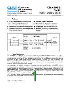
GMSK Packet Data Modem
CMX909B
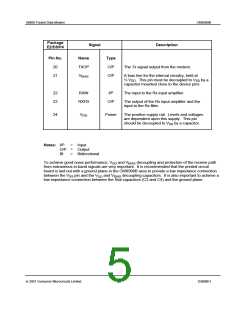
Package
E2/D5/P4
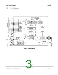
Signal
Description
Pin No.
20
Name
Type
O/P
TXOP
The Tx signal output from the modem.
21
V
BIAS
O/P
A bias line for the internal circuitry, held at
½ V . This pin must be decoupled to V by a
DD
SS
capacitor mounted close to the device pins.
22
23
RXIN
I/P
The input to the Rx input amplifier.
RXFB
O/P
The output of the Rx input amplifier and the
input to the Rx filter.
24
V
DD
Power
The positive supply rail. Levels and voltages
are dependent upon this supply. This pin
should be decoupled to V by a capacitor.
SS
Notes: I/P
=
=
=
Input
Output
Bidirectional
O/P
BI
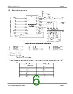
To achieve good noise performance, V and V
decoupling and protection of the receive path
BIAS
DD
from extraneous in-band signals are very important. It is recommended that the printed circuit
board is laid out with a ground plane in the CMX909B area to provide a low impedance connection
between the V pin and the V and V
decoupling capacitors. It is also important to achieve a
SS
BIAS
DD
low impedance connection between the Xtal capacitors (C3 and C4) and the ground plane.
ã 2001 Consumer Microcircuits Limited
5
D/909B/1

 CMLMICRO [ CML MICROCIRCUITS ]