GMSK Packet Data Modem
CMX909B
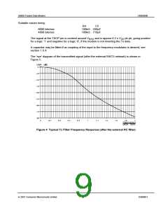
Figure 5 Transmitted Signal Eye Diagram (after the external RC filter)
1.5.1.13 Rx Level/Clock Extraction
These circuits, which operate only in receive mode, extract a bit rate clock from the received signal
and measure the received signal amplitude and dc offset. This information is then used to extract
the received bits and also to provide an input to the received Data Quality measuring circuit. The
external capacitors C6 and C7 form part of the received signal level measuring circuit.
1.5.1.14 Clock Oscillator and Dividers
This circuit derives the transmit bit rate (and the nominal receive bit rate) by frequency division of a
reference frequency which may be generated by the on-chip Xtal oscillator or applied from an
external source.
Note: If the on-chip xtal oscillator is to be used, then the external components X1, C3, C4 and R3
are required. If an external clock source is to be used, then it should be connected to the
XTAL/CLOCK input pin, the XTALN pin should be left unconnected, and X1, C3, C4 and R3 not
fitted.
1.5.1.15 Scramble/De-scramble
This block may be used to scramble/de-scramble the transmitted/received data blocks. It does this
by modulating the data with a 511-bit pseudorandom sequence, as described in section 1.5.5.4.
Scrambling smoothes the transmitted spectrum, especially when repetitive sequences are to be
transmitted.
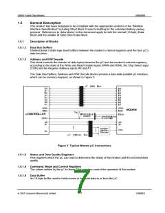
1.5.2
Modem - µC Interaction
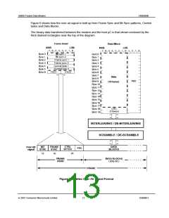
In general, data is transmitted over air in the form of messages, or ‘Frames’, consisting of a ‘Frame
Head’ optionally followed by one or more formatted data blocks. The Frame Head includes a Frame
Synchronisation pattern designed to allow the receiving modem to identify the start of a frame. The
following data blocks are constructed from the ‘raw’ data using a combination of CRC (Cyclic
Redundancy Checksum) generation, Forward Error Correction coding, Interleaving and Scrambling.
Details of the message formats handled by this modem are given in section 1.5.3.
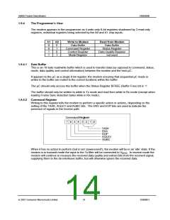
To reduce the processing load on the host µC, this modem has been designed to perform as much
as possible of the computationally intensive work involved in Frame formatting and de-formatting
and (when in receive mode) in searching for and synchronising onto the Frame Head. In normal
operation the modem will only require servicing by the µC once per received or transmitted data
block.
Thus, to transmit a block, the host µC has only to load the unformatted (raw) binary data into the
modem's data buffer then instruct the modem to format and transmit that data. The modem will then
ã 2001 Consumer Microcircuits Limited
10
D/909B/1

 CMLMICRO [ CML MICROCIRCUITS ]