Telephone Signalling Transceiver / Least Cost Router
CMX860
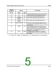
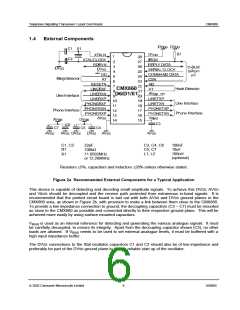
1.3
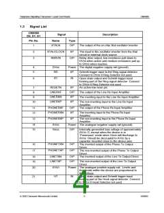
Signal List
CMX860
D6, D1, E1
Signal
Name
Description
Pin No.
Type
XTALN
XTAL/CLOCK
RDRVN
O/P
The output of the on-chip Xtal oscillator inverter.
1
I/P
2
3
The input to the oscillator inverter from the Xtal
circuit or external clock source.
Relay drive output, low resistance pull down to
DVSS when active and medium resistance pull up
to DVDD when inactive.
O/P
DVSS
RD
Power
I/P
4
5
The digital negative supply rail (ground).
Schmitt trigger input to the Ring signal detector.
Connect to DVSS if Ring Detector not used.
Open drain output and Schmitt trigger input
forming part of the Ring signal detector. Connect
to DVDD if Ring Detector not used.
RT
BI
6
RESETN
LINERXF
LINERXN
LINERXP
I/P
O/P
I/P
An active-low reset pin.
7
8
The output of the Line Rx Input Amplifier.
9
The inverting input to the Line Rx Input Amplifier.
I/P
10
The non-inverting input to the Line Rx Input
Amplifier.
PHONERXF
PHONERXN
O/P
I/P
The output of the Phone Rx Input Amplifier.
11
12
The inverting input to the Phone Rx Input
Amplifier.
PHONERXP
I/P
The non-inverting input to the Phone Rx Input
Amplifier.
13
AVSS
VBIAS
Power
O/P
14
15
The analogue negative supply rail (ground).
Internally generated bias voltage of approximately
AVDD /2, except when the device is in
‘Powersave’ mode when VBIAS will discharge to
AVSS. Should be decoupled to AVSS by a
capacitor mounted close to the device pins.
The inverted output of the Phone Tx Output
Driver.
PHONETXN
PHONETXP
O/P
O/P
16
17
The non-inverted output of the Phone Tx Output
Driver.
LINETXN
LINETXP
O/P
O/P
The inverted output of the Line Tx Output Driver.
18
19
The non-inverted output of the Line Tx Output
Driver.
AVDD
HT
Power The analogue positive supply rail. Levels and
thresholds within the device are proportional to
this voltage.
20
21
BI
Open drain output and Schmitt trigger input
forming part of the Hook signal detector. Connect
to DVDD if Hook Detector not used.
ã 2002 Consumer Microcircuits Limited
6
D/860/5

 CMLMICRO [ CML MICROCIRCUITS ]