P r o d u c t I n n o v a t i o n F r o m
PA119CE • PA119CEA
1. The current handling capability of the MOSFET geometry
and the wire bonds.
2. The junction temperature of the output MOSFETs.
GENERAL
Please read Application Note 1 "General Operating Con-
siderations" which covers stability, supplies, heat sinking,
mounting, current limit, SOA interpretation, and specification
interpretation. Visit www.Cirrus.com for design tools that help
automatetaskssuchascalculationsforstability,internalpower
dissipation, current limit; heat sink selection; Apex Precision
Power’scompleteApplicationNoteslibrary;TechnicalSeminar
Workbook; and Evaluation Kits.
The SOA curves combine the effect of these limits and allow
for internal thermal delays. For a given application, the direc-
tion and magnitude of the output current should be calculated
or measured and checked against the SOA curves. This is
simple for resistive loads but more complex for reactive and
EMF generating loads. The following guidelines may save
extensive analytical efforts:
CURRENT LIMIT
1. Capacitiveandinductiveloadsuptothefollowingmaximums
are safe:
Q2 (and Q25) limit output current by turning on and remov-
ing gate drive when voltage on pin 2 (pin 7) exceeds .65V dif-
ferential from the positive (negative) supply rail. With internal
resistors equal to 1.2Ω, current limits are approximately 0.5A
with no external current limit resistors. With the addition of
external resistors current limit will be:
±±S
CAPACITI±E LOAD
INDUCTI±E LOAD
40V
30V
20V
15V
.1µF
500µF
2500µF
∞
11mH
24mH
75mH
100mH
.65V
RCL
ILIM
=
+.54A
2. Safe short circuit combinations of voltage and current are
limited to a power level of 100W.
3. The output stage is protected against transient flyback.
However, for protection against sustained, high energy
flyback, external fast-recovery diodes should be used.
To determine values of external current limit resistors:
.65V
RCL
=
ICL – .54A
PHASE COMPENSATION
At low gain settings, an external compensation capacitor is
required to insure stability.In addition to the resistive feedback
network, roll off or integrating capacitors must also be consid-
ered when determining gain settings.The capacitance values
listed in the external connection diagram, along with good
high frequency layout practice, will insure stability. Interpolate
values for intermediate gain settings.
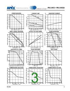
SUPPLY CURRENT
The PA119 features a class A/B driver stage to charge and
discharge gate capacitance of Q7 and Q19.As these currents
approach 0.5A, the savings of quiescent current over that of a
class A driver stage is considerable. However, supply current
drawn by the PA119, even with no load, varies with slew rate
of the output signal as shown below.
SUPPLY CURRENT
SAFE OPERATING AREA (SOA)
400
The MOSFET output stage of this power operational ampli-
fier has two distinct limitations:
VOUT = 60VP-P SINE
RL = 500 Ω
300
200
100
0
SOA
10
5
4
30K 100K 300K
1M
3M 10M
FREQUENCY, F (Hz)
3
OUTPUT LEADS
Keep the output leads as short as possible. In the video
frequency range, even a few inches of wire have significant
inductances, raising the interconnection impedance and limit-
ing the output current slew rate. Furthermore, the skin effect
increases the resistance of heavy wires at high frequencies.
Multistrand Litz Wire is recommended to carry large video
currents with low losses.
2
TC=25°C
1
10
20
30
40 50
80 100
INTERNAL VOLTAGE DROP SUPPLYTO OUTPUT, VS-VO (V)
4
PA119U

 CIRRUS [ CIRRUS LOGIC ]