CS42416
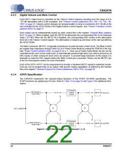
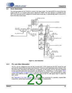
4.4
Clock Generation
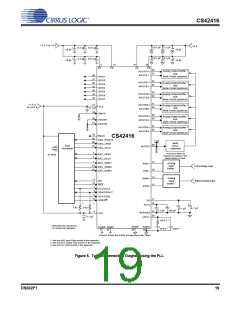
The clock generation for the CS42416 is shown in the figure below. The internal MCLK is derived from the
output of the PLL or a master clock source attached to OMCK. The mux selection is controlled by the
SW_CTRLx bits and can be configured to manual switch mode only, or automatically switch on loss of PLL
lock to the other source input.
RMCK_DIVx bits
00
2
01
RMCK
4
10
11
single
speed
X2
Internal
MCLK
256
00
01
10
DAC_LRCK
double
speed
ADC_LRCK
(slave mode)
00
01
PLL (256Fs)
8.192 -
Auto Detect
Input Clock
1,1.5, 2, 4
128
49.152 MHz
DAC_FMx bits
quad
speed
DAC_OLx
or ADC_OLx bits
PLL_LRCK bit
00
SW_CTRLx bits
(manual or auto
switch)
64
01
10
OMCK
not OLM
OLM #1
128FS
256FS
single
speed
DAC_SCLK
OLM #2
4
double
speed
00
01
10
2
ADC_LRCK
quad
speed
1
ADC_FMx bits
ADC_OLx and
ADC_SP SELx bits
00
01
10
not OLM
OLM #1
128FS
256FS
ADC_SCLK
OLM #2
Figure 10. Clock Generation
4.4.1
PLL and Jitter Attenuation
The PLL can be configured to lock onto the incoming ADC_LRCK signal from the ADC Serial Port and
generate the required internal master clock frequency. There are some applications where low jitter in the
recovered clock, presented on the RMCK pin, is important. For this reason, the PLL has been designed
to have good jitter-attenuation characteristics. By setting the PLL_LRCK bit to a ‘1’ in the register “Clock
Control (address 06h)” on page 48, the PLL will lock to the incoming ADC_LRCK and generate an output
master clock (RMCK) of 256Fs. Table 2 shows the output of the PLL with typical input Fs values for
ADC_LRCK.
See “Appendix B: PLL Filter” on page 62 for more information concerning PLL operation, required filter
components, optimal layout guidelines, and jitter-attenuation characteristics.
DS602F1
23

 CIRRUS [ CIRRUS LOGIC ]