CS42416
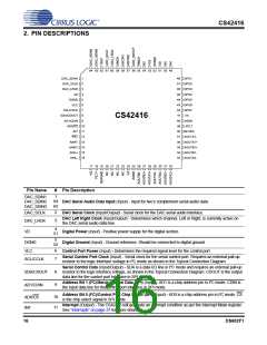
Reset (Input) - The device enters a low power mode and all internal registers are reset to their default
settings when low.
12
RST
13
14
AINR-
AINR+
Differential Right Channel Analog Input (Input) - Signals are presented differentially to the delta-sigma
modulators via the AINR+/- pins.
15
16
AINL+
AINL-
Differential Left Channel Analog Input (Input) - Signals are presented differentially to the delta-sigma
modulators via the AINL+/- pins.
17
18
19
VQ
Quiescent Voltage (Output) - Filter connection for internal quiescent reference voltage.
Positive Voltage Reference (Output) - Positive reference voltage for the internal sampling circuits.
Reference Ground (Input) - Ground reference for the internal sampling circuits.
FILT+
REFGND
36,37
35,34
32,33
31,30
28,29
27,26
AOUTA1 +,-
AOUTB1 +,-
AOUTA2 +,-
AOUTB2 +,-
AOUTA3 +,-
AOUTB3 +,-
Differential Analog Output (Output) - The full-scale differential analog output level is specified in the
Analog Characteristics specification table.
24
41
VA
Analog Power (Input) - Positive power supply for the analog section.
25
40
AGND
Analog Ground (Input) - Ground reference. Should be connected to analog ground.
Mute Control (Output) - The Mute Control pin outputs high impedance following an initial power-on con-
dition or whenever the PDN bit is set to a ‘1’, forcing the codec into power-down mode. The signal will
remain in a high impedance state as long as the part is in power-down mode. The Mute Control pin goes
to the selected “active” state during reset, muting, or if the master clock to left/right clock frequency ratio
is incorrect. This pin is intended to be used as a control for external mute circuits to prevent the clicks
and pops that can occur in any single supply system. The use of external mute circuits are not manda-
tory but may be desired for designs requiring the absolute minimum in extraneous clicks and pops.
38
MUTEC
LPFLT
39
PLL Loop Filter (Output) - An RC network should be connected between this pin and ground.
42
43
44
45
46
47
48
GPO7
GPO6
GPO5
GPO4
GPO3
GPO2
GPO1
General Purpose Output (Output) - These pins can be configured as general purpose output pins, an
ADC overflow interrupt or Mute Control outputs according to the General Purpose Pin Control registers.
53
VLS
Serial Port Interface Power (Input) - Determines the required signal level for the serial port interfaces.
Recovered Master Clock (Output) - Recovered master clock output from the External Clock Reference
(OMCK, pin 59) or the PLL which is locked to the incoming ADC_LRCK.
55
RMCK
ADC Serial Data Output (Output) - Output for two’s complement serial audio PCM data from the output
of the internal and external ADCs.
56
ADC_SDOUT
External ADC Serial Input (Input) - The CS42416 provides for up to two external stereo analog to digital
converter inputs to provide a maximum of six channels on one serial data output line when the CS42416
is placed in One-Line Mode.
58
57
ADCIN1
ADCIN2
External Reference Clock (Input) - External clock reference that must be within the ranges specified in
the register “OMCK Frequency (OMCK Freqx)” on page 48.
59
60
OMCK
ADC Left/Right Clock (Input/Output) - Determines which channel, Left or Right, is currently active on
the ADC serial audio data line.
ADC_LRCK
61
62
ADC_SCLK
TEST
ADC Serial Clock (Input/Output) - Serial clock for the ADC serial audio interface.
Test Pin (Input) - This pin must be connected to DGND.
DS602F1
17

 CIRRUS [ CIRRUS LOGIC ]