CS4365
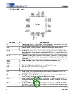
Pin Name
#
Pin Description
VQ
21 Quiescent Voltage (Output) - Filter connection for internal quiescent voltage. VQ
must be capacitively coupled to analog ground, as shown in the Typical Connection
Diagram. The nominal voltage level is specified in the Analog Characteristics and
Specifications section. VQ presents an appreciable source impedance and any cur-
rent drawn from this pin will alter device performance. However, VQ can be used to
bias the analog circuitry assuming there is no AC signal component and the DC cur-
rent is less then the maximum specified in the Analog Characteristics and Specifica-
tions section.
FILT+
20 Positive Voltage Reference (Output) - Positive reference voltage for the internal
sampling circuits. Requires the capacitive decoupling to analog ground as shown in
the Typical Connection Diagram.
AOUTA1 +,-
AOUTB1 +,-
AOUTA2 +,-
AOUTB2 +,-
AOUTA3 +,-
AOUTB3 +,-
39,40 Differential Analog Output (Output) - The full scale differential analog output level is
37,38 specified in the Analog Characteristics specification table.
35,36
33,34
29,30
27,28
MUTEC1
MUTEC2
MUTEC3
MUTEC4
MUTEC5
MUTEC6
41 Mute Control (Output) - The Mute Control pins go high during power-up initialization,
26 reset, muting, power-down or if the master clock to left/right clock frequency ratio is
25 incorrect. These pins are intended to be used as a control for external mute circuits on
24 the line outputs to prevent the clicks and pops that can occur in any single supply sys-
23 tem. Use of Mute Control is not mandatory but recommended for designs requiring
22 the absolute minimum in extraneous clicks and pops.
Hardware Mode Definitions
Mode Selection (Input) - Determines the operational mode of the device as detailed in Tables
6 and 7.
M0
M1
M2
M3
M4
17
16
15
12
10
Software Mode Definitions
SCL/CCLK
15 Serial Control Port Clock (Input) - Serial clock for the serial control port. Requires an
2
external pull-up resistor to the logic interface voltage in I C mode as shown in the
Typical Connection Diagram.
2
SDA/CDIN
16
Serial Control Port Data (Input/Output) - SDA is a data I/O line in I C mode and is
open drain, requiring an external pull-up resistor to the logic interface voltage, as
shown in the Typical Connection Diagram; CDIN is the input data line for the control
port interface in SPI mode.
2
AD0/CS
17
Address Bit 0 (I C) / Control Port Chip Select (SPI) (Input) - AD0 is a chip address
2
pin in I C mode; CS is the chip select signal for SPI mode.
TST
10, 12 Test - These pins need to be tied to analog ground.
DSD Definitions
Direct Stream Digital Input (Input) - Input for Direct Stream Digital serial audio data.
DSD Serial Clock (Input) - Serial clock for the Direct Stream Digital serial audio interface.
DSDA1
DSDB1
DSDA2
DSDB2
DSDA3
DSDB3
3
2
1
48
47
46
DSD_SCLK
42
DS670PP1
7

 CIRRUS [ CIRRUS LOGIC ]