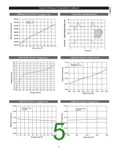
Electrical Characteristics: 0¡C ² TA ² 70¡C, 0¡C ² TJ ² 150¡C, VSENSE = VOUT and VAdj = 0V unless otherwise specified.
PARAMETER
TEST CONDITIONS
MIN
TYP
MAX
UNIT
VPOWER Supply Only
Output Current
VPOWER = 6V, VCONTROL not connected,
VADJUST = VOUT = VSENSE = 0V
0.1
1
mA
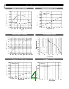
Note 1: The minimum load current is the minimum current required to maintain regulation. Normally the current in the resistor
divider used to set the output voltage is selected to meet the minimum load current requirement.
Note 2: The control pin current is the drive current required for the output transistor. This current will track output
current with roughly a 1:100 ratio. The minimum value is equal to the quiescent current of the device.
Note 3: This parameter is guaranteed by design and is not 100% production tested.
Note 4: Dropout is defined as either minimum control voltage (VCONTROL) or minimum power voltage (VPOWER) to output volt-
age differential required to maintain 1.5% regulation at a particular load current.
Note 5: This parameter is guaranteed by design, but not parametrically tested in production. However, a 100% thermal shutdown
functional test is performed on each part.
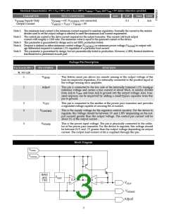
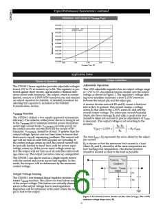
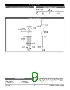
Package Pin Description
PACKAGE PIN #
PIN SYMBOL
FUNCTION
5L TO-220
1
VSENSE
This Kelvin sense pin allows for remote sensing of the output voltage at the
load for improved regulation. It is internally connected to the positive input of
the voltage sensing error amplifier.
2
Adjust
This pin is connected to the low side of the internally trimmed 1.5% bandgap
reference voltage and carries a bias current of about 50uA. A resistor divider
from Adj to VOUT and from Adj to ground sets the output voltage. Also, tran-
sient response can be improved by adding a small bypass capacitor from this
pin to ground.
3
4
VOUT
This pin is connected to the emitter of the power pass transistor and provides
a regulated voltage capable of sourcing 8A of current.
VCONTROL
This is the supply voltage for the regulator control circuitry. For the device to
regulate, this voltage should be between 1V and 1.30V (depending on the out-
put current) greater than the output voltage. The control pin current will be
about 1% of the output current .
5
VPOWER
This is the power input voltage. The pin is physically connected to the collec-
tor of the power pass transistor. For the device to regulate, this voltage should
be between 0.1V and .7V greater than the output voltage depending on output
current. The output load current of 8A is supplied through this pin.
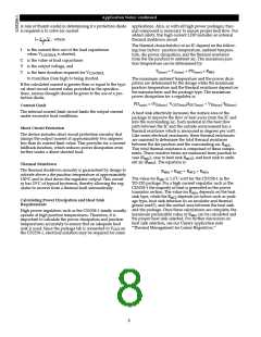
Block Diagram
VPOWER
VCONTROL
BIAS
and
TSD
VREF
-
+
+
EA
IA
-
VOUT
VSENSE
Adjust
3

 CHERRY [ CHERRY SEMICONDUCTOR CORPORATION ]