Applications Information: continued
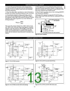
Trace 3 = V
(10V/div.)
GATE(H)
Trace 3 = 12V Input (V
Trace 4 = 5V Input (2V/div.)
Trace 1 = Regulator Output Voltage (1V/div.)
Trace 2 = Power Good Signal (2V/div.)
) and V
) (10V/div.)
CC1
CC2
Math 1= V
- 5V
GATE(H)
IN
Trace 4 = V
Trace 2 = Inductor Switching Node (5V/div.)
(10V/div.)
GATE(L)
Figure 17: CS5155H gate drive waveforms depicting rail to rail swing.
Figure 16: CS5155H demonstration board during power up. Power Good
signal is activated when output voltage reaches 1.70V.
The most important aspect of MOSFET performance is
RDSON, which effects regulator efficiency and MOSFET
thermal management requirements.
Selecting External Components
The CS5155H can be used with a wide range of external
power components to optimize the cost and performance of
a particular design. The following information can be used
as general guidelines to assist in their selection.
The power dissipated by the MOSFETs may be estimated
as follows;
Switching MOSFET:
Power = ILOAD2 × RDSON × duty cycle
NFET Power Transistors
Both logic level and standard MOSFETs can be used. The
reference designs derive gate drive from the 12V supply
which is generally available in most computer systems and
utilize logic level MOSFETs. A charge pump may be easily
implemented to support 5V or 12V only systems (maximum
of 20V). Multiple MOSFETs may be paralleled to reduce
losses and improve efficiency and thermal management.
Synchronous MOSFET:
Power = ILOAD2 × RDSON × (1 - duty cycle)
Duty Cycle =
VOUT + (ILOAD × RDSON OF SYNCH FET
)
VIN + (ILOAD × RDSON OF SYNCH FET) - (ILOAD × RDSON OF SWITCH FET
)
Voltage applied to the MOSFET gates depends on the
application circuit used. Both upper and lower gate driver
outputs are specified to drive to within 1.5V of ground
when in the low state and to within 2V of their respective
bias supplies when in the high state. In practice, the MOS-
FET gates will be driven rail to rail due to overshoot caused
by the capacitive load they present to the controller IC. For
the typical application where VCC1 = VCC2 = 12V and 5V is
used as the source for the regulator output current, the fol-
lowing gate drive is provided;
Off Time Capacitor (COFF
)
The COFF timing capacitor sets the regulator off time:
TOFF = COFF × 4848.5
When the VFFB pin is less than 1V, the current charging the
COFF capacitor is reduced. The extended off time can be cal-
culated as follows:
TOFF = COFF × 24,242.5.
VGATE(H) = 12V - 5V = 7V, VGATE(L) = 12V (see Figure 17).
Off time will be determined by either the TOFF time, or the
time out timer, whichever is longer.
The preceding equations for duty cycle can also be used to
calculate the regulator switching frequency and select the
11

 CHERRY [ CHERRY SEMICONDUCTOR CORPORATION ]