Data Sheet
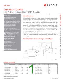
CLC1003 SOT23-5 Pin Assignments
CLC1003 SOT Pin Configuration
Pin No.
Pin Name
OUT
Description
1
2
3
4
5
Output
OUT
1
2
3
5
4
+V
S
-V
Negative supply
Positive input
Negative input
Positive supply
S
-V
S
+
-
+IN
-IN
-IN
+IN
+V
S
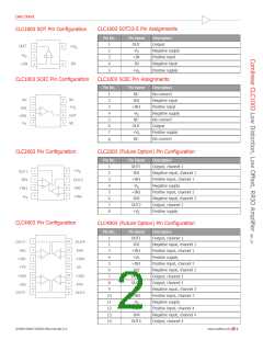
CLC1003 SOIC Pin Assignments
CLC1003 SOIC Pin Configuration
Pin No.
Pin Name
NC
Description
No connect
Negative input
Positive input
Negative supply
No connect
Output
1
2
3
4
5
6
7
1
2
3
4
8
7
NC
+V
NC
-IN1
-IN1
+IN1
S
-V
S
6
5
OUT
NC
+IN1
NC
-V
S
OUT
+V
Positive supply
No connect
S
NC
8
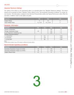
CLC2003 Pin Configuration
CLC2003 (Future Option) Pin Configuration
Pin No.
Pin Name
OUT1
-IN1
Description
1
2
3
4
5
6
7
8
Output, channel 1
Negative input, channel 1
Positive input, channel 1
Negative supply
1
2
3
4
8
7
+V
S
OUT1
-IN1
+IN1
OUT2
-IN2
-V
S
6
5
+IN1
+IN2
-IN2
Positive input, channel 2
Negative input, channel 2
Output, channel 2
Positive supply
+IN2
-V
S
OUT2
+V
S
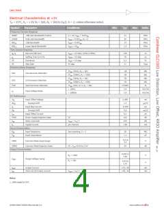
CLC4003 Pin Configuration
CLC4003 (Future Option) Pin Configuration
Pin No.
Pin Name
OUT1
-IN1
Description
1
2
Output, channel 1
1
2
3
4
14
13
12
11
10
9
OUT1
-IN1
OUT4
-IN4
Negative input, channel 1
Positive input, channel 1
Positive supply
3
+IN1
4
+V
S
+IN1
+VS
+IN4
-VS
5
+IN2
-IN2
Positive input, channel 2
Negative input, channel 2
Output, channel 2
6
5
6
7
+IN2
+IN3
-IN3
7
OUT2
OUT3
-IN3
8
Output, channel 3
-IN2
9
Negative input, channel 3
Positive input, channel 3
Negative supply
8
OUT2
OUT3
10
11
12
13
14
+IN3
-V
S
+IN4
-IN4
Positive input, channel 4
Negative input, channel 4
Output, channel 4
OUT4
©2004-2008 CADEKA Microcircuits LLC
www.cadeka.com
2

 CADEKA [ CADEKA MICROCIRCUITS LLC. ]