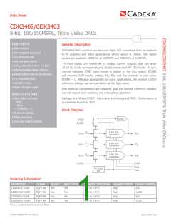
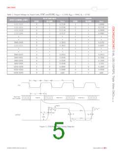
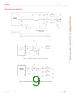
Data Sheet
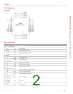
Pin Configuration
TQFP-48
1
2
3
4
5
6
7
8
36
35
34
33
32
31
30
29
28
27
26
25
GND
G0
G1
G2
G3
G4
G5
G6
G7
R
V
REF
REF
COMP
IO
IO
R
G
TQFP
CDK3402/3403
V
V
DD
DD
IO
B
9
GND
GND
CLOCK
NC
BLANK
SYNC
10
11
12
V
DD
Pin Assignments
Pin No.
Pin Name
Description
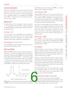
Clock Input
cꢀꢁꢂk ꢃꢄd pꢅxꢆꢀ i/o
26
47-40
CLK
R7-0
G7-0
B7-0
Red Pixel Data Inputs
Green Pixel Data Inputs
Blue Pixel Data Inputs
9–2
23–16
cꢁꢄꢇꢈꢁꢀꢉ
11
Sync Pulse Input
Blanking Input
SYNC
10
BLANK
Vꢅdꢆꢁ oꢊꢇꢋꢊꢇꢉ
Red Current Output
Green Current Output
Blue Current Output
33
32
29
IOR
IOG
IOB
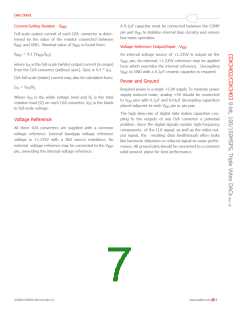
Vꢁꢀꢇꢃgꢆ rꢆꢌꢆꢈꢆꢄꢂꢆ
35
36
34
V
Voltage Reference Output/Input
REF
R
Current-Setting Resistor
Compensation Capacitor
REF
COMP
pꢁwꢆꢈ ꢃꢄd Gꢈꢁꢊꢄd
12, 30, 31
V
Power Supply
Ground
DD
1, 14, 15,
27, 28, 38,
39, 48
GND
NC
13, 24, 25,
37
No Connect
©2008 CADEKA Microcircuits LLC
www.cadeka.com
2

 CADEKA [ CADEKA MICROCIRCUITS LLC. ]