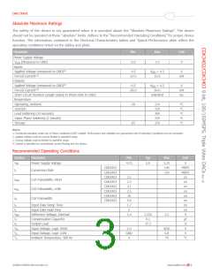
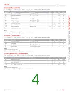
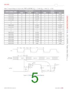
Data Sheet
regulated and free of high-frequency noise. Careful power
supply decoupling will ensure the highest quality video
signals at the output of the circuit. The CDK3402/3403 has
separate analog and digital circuits. To keep digital system
noise from the D/A converter, it is recommended that
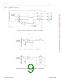
Applications Dicussion
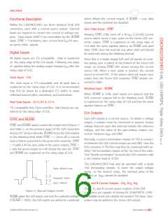
Figure 9 below illustrates a typical CDK3402/3403 interface
circuit. In this example, an optional 1.2V bandgap refer-
ence is connected to the V
output, overriding the inter-
REF
nal voltage reference source.
power supply voltages (V ) come from the system analog
DD
power source and all ground connections (GND) be made
to the analog ground plane. Power supply pins should be
Grounding
It is important that the CDK3402/3403 power supply is well- individually decoupled at the pin.
+5V
10µF
0.1µF
Red
o
75Ω
75Ω
75Ω
VDD
GND
Z
= 75Ω
IOR
IOG
IOB
RED PIXEL
INPUT
R7-0
G7-0
B7-0
Green w/Sync
75Ω
75Ω
75Ω
Z
= 75Ω
o
Blue
GREEN PIXEL
INPUT
Z
= 75Ω
o
CDK3402/3403
Triple 8-bit D/A Converter
BLUE PIXEL
INPUT
+5V
COMP
CLOCK
SYNC
CLK
3.3kΩ
0.1µF
(not required without external reference)
SYNC
BLANK
VREF
RREF
BLANK
0.1µF
LM185-1.2
(Optional)
590Ω
Figure 9. Typical Interface Circuit Diagram
3. The ground plane should be solid, not cross-hatched.
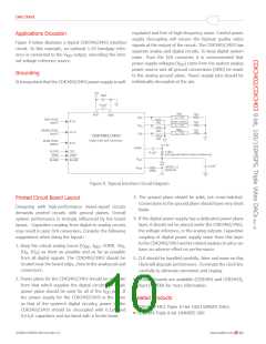
Printed Circuit Board Layout
Connections to the ground plane should have very short
leads.
Designing with high-performance mixed-signal circuits
demands printed circuits with ground planes. Overall
system performance is strongly influenced by the board
layout. Capacitive coupling from digital to analog circuits
may result in poor D/A conversion. Consider the following
suggestions when doing the layout:
4. If the digital power supply has a dedicated power plane
layer, it should not be placed under the CDK3402/3403,
the voltage reference, or the analog outputs. Capacitive
coupling of digital power supply noise from this layer
to the CDK3402/3403 and its related analog circuitry can
have an adverse effect on performance.
1. Keep the critical analog traces (V , I , COMP, IO ,
REF REF
S
IO , IO ) as short as possible and as far as possible
R
G
from all digital signals. The CDK3402/3403 should be
located near the board edge, close to the analog out-put
connectors.
5. CLK should be handled carefully. Jitter and noise on this
clock will degrade performance. Terminate the clock line
carefully to eliminate overshoot and ringing.
2. Power plane for the CDK3402/3403 should be separate
from that which supplies the digital circuitry. A single
Evaluation boards are available (CEB3402 and CEB3403),
contact CADEKA for more information.
power plane should be used for all of the V pins. If
DD
the power supply for the CDK3402/3403 is the same
as that of the system’s digital circuitry, power to the
CDK3402/3403 should be decoupled with 0.1µF and
0.01µF capacitors and iso-lated with a ferrite bead.
Related Products
n
ꢀ
CDK3400/3401 Triple 10-bit 100/150MSPS DACs
CDK3404 Triple 8-bit 180MSPS DAC
n
ꢀ
©2008 CADEKA Microcircuits LLC
www.cadeka.com
10

 CADEKA [ CADEKA MICROCIRCUITS LLC. ]