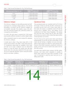
Data Sheet
Digital and Timing Electrical Characteristics
(AVDD = 1.8V, DVDD = 1.8V, DVDDCLK = 1.8V, OVDD = 2.5V, 20/40/65/80MSPS clock, 50% clock duty cycle,
-1 dBFS input signal, 5pF capacitive load, unless otherwise noted)
Symbol
Parameter
Conditions
Min
Typ
Max
Units
Clock Inputs
Duty Cycle
Compliance
20
80
% high
CMOS, LVDS, LVPECL, Sine Wave
400
1.6
mV
Differential input swing
pp
Input Range
Vpp
V
Differential input swing, sine wave clock input
Keep voltages within ground and voltage of OVDD
Differential
Input Common Mode Voltage
Input Capacitance
0.3
VOVDD -0.3
2
pF
Timing
TPD
Start Up Time from Power Down
From Power Down Mode to Active Mode
From Sleep Mode to Active Mode
900
clk cycles
TSLP
TOVR
TAP
Start Up Time from Sleep
Out Of Range Recovery Time
Aperture Delay
clk cycles
clk cycles
ns
20
1
0.8
<0.5
12
εRMS
TLAT
Aperture Jitter
ps
Pipeline Delay
clk cycles
ns
5pF load on output bits (see timing diagram)
See timing diagram
3
10
TD
Output Delay
TDC
Output Delay Relative to CLK_EXT
1
ns
6
Logic Inputs
VOVDD ≥ 3.0V
2
V
V
VIH
VIL
High Level Input Voltage
Low Level Input Voltage
VOVDD = 1.7V – 3.0V
VOVDD ≥ 3.0V
0.8 • VOVDD
0
0.8
0.2 • VOVDD
10
V
VOVDD = 1.7V – 3.0V
0
V
IIH
High Level Input Leakage Current
Low Level Input Leakage Current
Input Capacitance
-10
-10
μA
μA
pF
IIL
10
CI
3
Logic Outputs
VOH
VOL
High Level Output Voltage
Low Level Output Voltage
-0.1 +VOVDD
V
V
0.1
5
Post-driver supply voltage equal to pre-driver
supply voltage VOVDD = VVDVDD
Post-driver supply voltage above 2.25V (1)
pF
CL
Max Capacitive Load
10
pF
Note:
(1) The outputs will be functional with higher loads. However, it is recommended to keep the load on output data bits as low as possible to keep dynamic currents
and resulting switching noise at a minimum.
©2009 CADEKA Microcircuits LLC
www.cadeka.com
10

 CADEKA [ CADEKA MICROCIRCUITS LLC. ]