Data Sheet
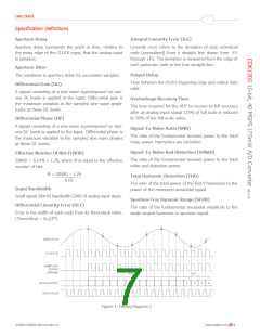
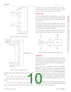
a specific case. V
of 4.0V is applied to V , and V
RHF RLF
REF
is tied to AGND. A 90mV drop is seen at V
(= 3.91V),
RHS
and a 75mV increase is seen at V
(= 0.075V).
RLS
Analog Input
V
V
is the analog input. The input voltage range is from
IN
to V
(typically 4.0V) and will scale proportionally
RLS
RHS
with respect to the voltage reference. (See Voltage Refer-
ence section.)
The drive requirements for the analog inputs are very
minimal when compared to most other converters due to
the CDK1305 extremely low input capacitance of only 5pF
and very high input resistance of 50kΩ.
The analog input should be protected through a series
resistor and diode clamping circuit as shown in Figure 7.
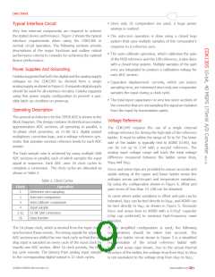
Figure 4. Ladder Force/Sense Circuit
Figure 6. Recommended Input Protection Circuit
Calibration
The CDK1305 uses an auto-calibration scheme to ensure
10-bit accuracy over time and temperature. Gain and
offset errors are continually adjusted to 10-bit accuracy
during device operation. This process is completely trans-
parent to the user.
Upon powerup, the CDK1305 begins its calibration
algorithm. In order to achieve the calibration accuracy
required, the offset and gain adjustment step size is a
fraction of a 10-bit LSB. Since the calibration algorithm
is an oversampling process, a minimum of 10,000 clock
cycles are required. This results in a minimum calibration
time upon powerup of 250μs (for a 40MHz clock). Once
calibrated, the CDK1305 remains calibrated over time and
temperature.
Figure 5. Reference Ladder Circuit
Typically, the top side voltage drop for V
equal:
to V
will
will
RHF
RHS
V
– V
= 2.25 % of (V – V ) (typical)
RHF RLF
RHF
RHS
and the bottom side voltage drop for V
equal:
to V
RLF
RLS
Since the calibration cycles are initiated on the rising edge
of the clock, the clock must be continuously applied for
the CDK1305 to remain in calibration.
V
– V
= 1.9 % of (V
– V ) (typical)
RLS
RLF
RHF RLF
Figure 5 shows an example of expected voltage drops for
©2008 CADEKA Microcircuits LLC
www.cadeka.com
10

 CADEKA [ CADEKA MICROCIRCUITS LLC. ]