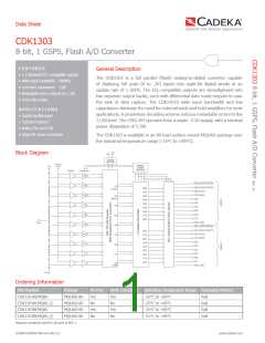
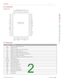
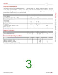
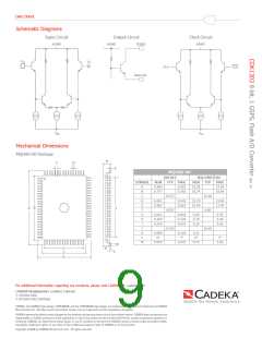
Data Sheet
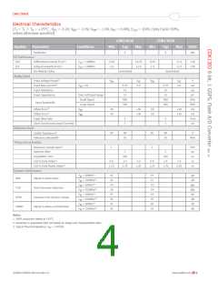
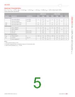
Electrical Characteristics
(T = T = T = +25°C , V = -5.2V, V = -2.0V, V = -1.0V, V = 0.00V, ƒ = 1GHz, Duty Cycle=50%,
J
C
A
EE
RB
RM
RT
CLK
unless otherwise specified)
cDK1303a
cDK1303B
symbꢀꢁ
pꢂꢃꢂmꢄꢅꢄꢃ
cꢀꢆdꢇꢅꢇꢀꢆꢈ
Mꢇꢆ
tyꢉ
Mꢂx
Mꢇꢆ
tyꢉ
Mꢂx
uꢆꢇꢅꢈ
Resolution
8
8
bits
DC Performance
DLE
ILE
Differential Linearity Error(1)
Integral Linearity Error(1)
No Missing Codes
ƒclk = 100MHz
ƒclk = 100MHz
-0.85
-1.0
+0.95
+1.0
-0.95
-1.5
+1.5
+1.5
LSB
LSB
Guaranteed
Guaranteed
Analog Input
Input Voltage Range(1)
Input Bias Current(1)
Input Resistance
VRB
VRT
2.0
VRB
VRT
2.0
V
VIN = 0V
0.75
15
0.75
15
mA
kΩ
Input Capacitance
Over Full Input Range
Small Signal
Large Signal
VRT
15
15
pF
900
500
900
500
MHz
MHz
mV
mV
V/ns
μA
Input Bandwidth
Offset Error(2)
Offset Error(2)
Input Slew Rate
-30
-30
+30
+30
-30
-30
+30
+30
VRB
5
2
5
2
Clock Synchronous Input Currents
Reference Input
Ladder Resistance(1)
Reference Bandwidth
60
1
80
30
60
1
80
30
Ω
MHz
Timing Characteristics
Maximum Sample Rate(1)
GHz
ps
Aperture Jitter
2
2
Acquisition Time
250
1.4
250
1.4
ps
CLK to Data Delay(2)
CLK to Data Ready Delay(2)
0.9
1.9
0.9
1.9
ns
1.25
1.75
2.25
1.25
1.75
2.25
ns
Dynamic Performance
ƒIN = 50MHz(1)
ƒIN = 250MHz(1)
ƒIN = 50MHz(1)
ƒIN = 250MHz(1)
ƒIN = 50MHz(1)
ƒIN = 250MHz(1)
ƒIN = 50MHz(1)
ƒIN = 250MHz(1)
45
43
43
41
dB
dB
SNR
Signal-to-Noise Ratio
-44
-36
47
-42
-34
43
dBc
dBc
dB
THD
Total Harmonic Distortion
Spurious Free Dynamic Range
Signal-to-Noise and Distortion
SFDR
SINAD
39
35
dB
42
40
dB
35
33
dB
nꢀꢅꢄꢈ:
1. 100% production tested at +25°C.
2. Parameter is guaranteed (but not tested) by design and characterization data.
3. Typical Thermal Impedance: θ = +4°C/W.
JC
©2008 CADEKA Microcircuits LLC
www.cadeka.com
4

 CADEKA [ CADEKA MICROCIRCUITS LLC. ]