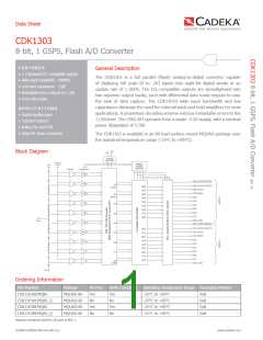
Data Sheet
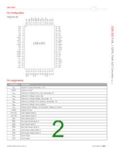
Typical Interface Circuit
V
, V , V , V , V (Reference Inputs)
RBF RBS RTF RTS RM
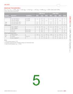
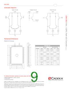
ThecircuitinFigure1isintendedtoshowthemostelaborate There are two reference inputs and one external reference
methodofachievingtheleasterrorbycorrectingforintegral voltage tap. These are -2V (V force and sense), midtap
RB
linearity, input induced distortion, and power supply/ (V ) and AGND (V force and sense). The reference pins
RM
RT
ground noise. This is achieved by the use of external and tap can be driven by op amps as shown in Figure 1 or
reference ladder tap connections, input buffer, and supply may be bypassed for limited temperature operation.
V
RM
decoupling. Please contact the factory for the CDK1303 These voltage inputs can be bypassed to AGND for further
evaluation board application note that contains more details noise suppression if so desired.
on interfacing the CDK1303. The function of each pin
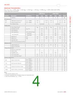
Table 1. Output Coding
and external connections to other components is as follows:
Vin
> -0.5 LSB
-0.5 LSB
D8
D7–D0
V , AGND, DGND
EE
1
10000000
1
0
10000000
10000000
VEE is the supply pin with AGND as ground for the device.
The power supply pins should be bypassed as close to the
device as possible with at least a 0.01μF ceramic capacitor.
A 10μF tantalum can also be used for low frequency
suppression. DGND is the ground for the ECL outputs and
is to be referenced to the output pulldown voltage and
appropriately bypassed as shown in Figure 1.
-1.5 LSB
0
0
10000000
10000001
•
•
•
•
•
•
•
•
•
> -1.0V
0
0
11000000
01000000
V
(Analog Input)
IN
•
•
•
•
•
•
•
•
•
There are two analog input pins that are tied to the same
point internally. Either one may be used as an analog in-
put sense and the other for input force. This is convenient
for testing the source signal to see if there is sufficient
drive capability. The pins can also be tied together and
driven by the same source. The CDK1303 is superior to
similar devices due to a preamplifier stage before the com-
parators. This makes the device easier to drive because it
has constant capacitance and induces less slew rate distortion.
-2.0V +0.5 LSB
0
0
00000001
00000000
< (-2.0V +0.5 LSB)
0
00000000
Indicates the transition between the two codes
Thermal Management
The typical thermal impedance is as follows:
= +17 °C/W in still air with no heat sink
CLK, CLK (Clock Inputs)
Θ
CA
The clock inputs are designed to be driven differentially
with ECL levels. The duty cycle of the clock should be kept
at 50% to avoid causing larger second harmonics. If this is
not important to the intended application, then duty cycles
other than 50% may be used.
We highly recommend that a heat sink be used for this
device with adequate air flow to ensure rated performance
of the device. We have found that a Thermalloy 17846
heat sink with a minimum air flow of 1 meter/second
(200 linear feet per minute) provides adequate thermal
performance under laboratory tests. Application specific
conditions should be taken into account to ensure that the
device is properly heat sinked.
D0 To D8, DR, DR, (A and B)
The digital outputs can drive 50Ω to ECL levels when pulled
down to -2V. When pulled down to -5.2V, the outputs can
drive 130Ω to 1kΩ loads. All digital outputs are grey code
with the coding as shown in Table 1. Cadeka recommends
using differential receivers on the outputs of the data ready
lines to ensure the proper output rise and fall times.
©2008 CADEKA Microcircuits LLC
www.cadeka.com
7

 CADEKA [ CADEKA MICROCIRCUITS LLC. ]