BL9110
1A Low Dropout, Low Quiescent Current
High PSRR CMOS Linear Regulator
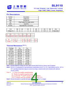
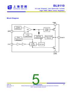
Pin Descriptions
Symbol
VOUT
GND
Description
Output Pin
Ground Pin
CE
VDD
Chip Enable Pin (High active)
Input Pin
ADJ/NC
Adjustable/No Connection
VVV
100
1.0
120
1.2
130
1.3
…
…
285
…
…
495
500
5.0
ADJ
Voltage (V)
2.85
4.95
Adjustable
Y
0
1
2
3
4
…
Year 2010 2011 2012 2013 2014 ……
W
Week
01
A
2
B
…
…
26 27 28
Z
…
…
52
Thermal Resistance (Note 4)
:
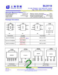
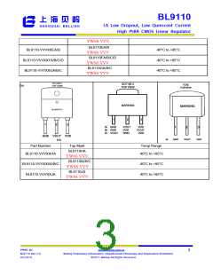
Package
DFN-6
ӨJA
ӨJC
95C/W
160C/W
90C/W
160C/W
90C/W
160C/W
65C/W
50C/W
180C/W
10C/W
45C/W
10C/W
20C/W
10C/W
20C/W
7C/W
SOT-89-5
TO-252-5
SOT-223-5
TO-252-3
SOT-223-3
TO-263-3
TO-220-3
SOT89-3
7C/W
50C/W
Note 1: Absolute Maximum Ratings are those values beyond which the life of a device may be impaired.
Note 2: The BL9110 is guaranteed to meet performance specifications from 0°C to 70°C. Specifications over the –40°C to
85°C operating temperature range are assured by design, characterization and correlation with statistical
process controls.
Note 3: Y: Year of assembly manufacturing
W: Week of assembly manufacturing
SS: Lot ID (the 7th and 8th number of Lot numbers)
VVV: Voltage code (for example 100 stands for 1.0V)
Note 4: Thermal Resistance is specified with approximately 1 square of 1 oz copper.
PPMIC BU
BL9110 Rev 2.0
04/2016
www.belling.com.cn
4
Belling Proprietary Information. Unauthorized Photocopy and Duplication Prohibited
© 2011 Belling All Rights Reserved

 BELLING [ BELLING ]