Shanghai Belling Corp., Ltd
BL55028
zip: 200233 Tel: 86-021-64850700 Fax: 86-021-64855865
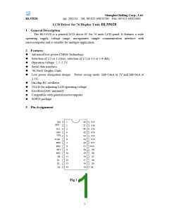
4 Pin Description
Pin No.
Pin name
Function
Serial data input/output
Serial clock input
SDA
SCI
2
3
Vdd
Supply voltage
4
Vss
Vlcd
ground
5
6
7-10
LCD supply voltage
Common terminal driving output
Segment terminal driving output
Com0、Com2、Com1、Com3
S0——S18
11-28、1
Tab.1
5 Function Description
1.function circuit
The BL550028 has all function circuits that can directly drive any static or multiplexed
LCD containing up to four commons and up to 19 segments. The function circuits
include:Power-on reset, LCD bias generator, LCD voltage selector, Oscillator, display RAM,
Timing, Display latch, Shift register, Common/segment outputs, input/output bank selector,
Blinker, Data pointer, etc.
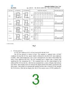
2.display function decription
The display RAM is a static 19x 4-bit RAM which stores LCD data. A logic 1 in the
RAM bit-map indicates the on state of the corresponding LCD segment; similarly, a logic 0
indicates the off state. There is a one-to-one correspondence between the RAM addresses and
the segment outputs, and between the individual bits of a RAM word and the common
outputs. (see Fig.2).
Display RAM address and SEGMENT(S0~S18)output
0
1
2
3
。
。
。
。
15 16 17
18
COM
(Com0~
Com3)
输出
0
1
2
3
Fig2
When display data is transmitted to the BL55028, the display bytes received are stored
in the display RAM in accordance with the selected LCD drive mode. To illustrate the filling
order, an example of a 7-segment numeric display showing all drive modes is given in Fig.3;
the RAM filling organization depicted applies equally to other LCD types.
2

 BELLING [ BELLING ]