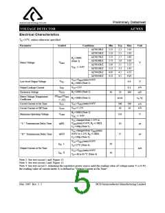
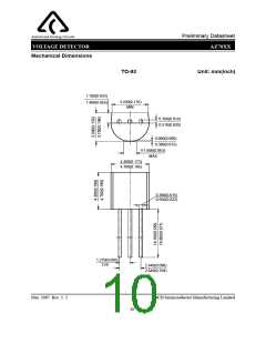
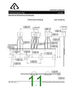
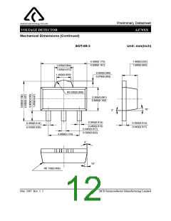
Preliminary Datasheet
VOLTAGE DETECTOR
AZ70XX
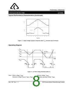
Operating Diagram (Continued)
Figure 12 is a typical timing waveform for AZ70XX.
typical). Below minimum operating voltage, the out-
put is undefined.
In normal steady-state operation when V >V
,
CC
DET-
the output will be in a logic high state and V
is
OUT
3. During power-up, V
will remain undefined until
OUT
dependent upon the voltage that the pull-up resistor
connected to.
V
rises above V
, at which time the output will
OPR
CC
become valid. V
will be in its active low state
OUT
Here is some explanations for AZ70XX's operation.
while
V
<V
<V
(V
=V
+V
).
HYS
OPR
CC
DET+
DET+
DET-
V
is the release voltage. V
means the hystere-
DET+
HYS
1. When the input voltage V falls below V
, the
DET-
CC
sis voltage and is the difference voltage between the
and V
output will pull down to logic low after a delay time of
tpHL. In general, at rated output current and V
V
.
DET-
DET+
,
CC
V
can be pulled down to a voltage as low as within
OUT
4. When V rises above V
, the output will be in
DET+
CC
0.4V from GND. (See the Electrical Characteristics
section). The voltage level V
its inactive state. After a delay time of tpLH, V
will be in its logic high state .
OUT
means the detect
DET-
voltage.
2. The output, V
, will stay valid until V falls
CC
OUT
below the minimum operating voltage, V
(0.8V
OPR
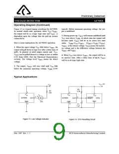
Typical Applications
VCC +5V
VCC
R1
3.3k
R1
220
1
1
VCC
VCC
VCC
CPU
GND
3
3
AZ70XX
OUT
AZ70XX
OUT
RESET
+
GND
2
GND
2
LED
C1
1 µF
Figure 13. Low Voltage Indicator
Figure 14. CPU Resetting Circuit
Mar. 2007 Rev. 1. 5
BCD Semiconductor Manufacturing Limited
9

 BCDSEMI [ BCD SEMICONDUCTOR MANUFACTURING LIMITED ]