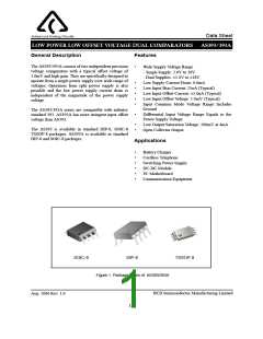
Data Sheet
LOW POWER LOW OFFSET VOLTAGE DUAL COMPARATORS
AS393/393A
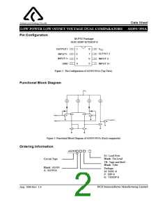
Pin Configuration
M /P/G Package
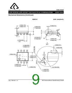
SOIC-8/DIP-8/TSSOP-8
1
8
OUTPUT1
VCC
7
7
OUTPUT 2
INPUT 2-
INPUT 2+
INPUT1-
INPUT1+
2
3
6
5
GND
4
Figure 2. Pin Configuration of AS393/393A (Top View)
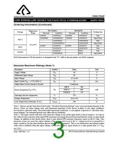
Functional Block Diagram
VCC
Q2
Q3
+INPUT
-INPUT
Q1
Q4
OUTPUT
Q8
Q7
Q5
Q6
Figure 3. Functional Block Diagram of AS393/393A (Each comparator)
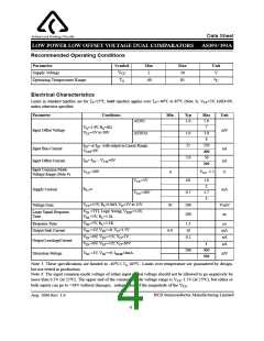
Ordering Information
-
AS393
E1: Lead Free
Blank: Tin Lead
Circuit Type
TR: Tape and Reel
Blank: Tube
Package
M: SOIC-8
P: DIP-8
Blank: AS393
A: AS393A
G: TSSOP-8
BCD Semiconductor Manufacturing Limited
Aug. 2006 Rev. 1.6
2

 BCDSEMI [ BCD SEMICONDUCTOR MANUFACTURING LIMITED ]