ꢀ ꢁꢂ ꢃ ꢄ ꢅ ꢆ
www.ti.com
SLES100 − DECEMBER 2003
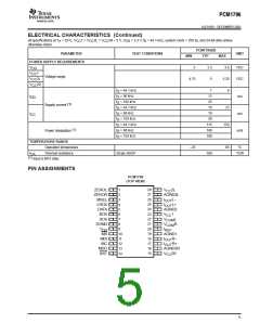
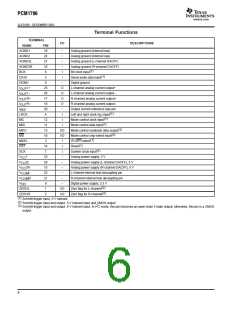
Terminal Functions
TERMINAL
I/O
DESCRIPTIONS
NAME
AGND1
AGND2
AGND3L
AGND3R
BCK
PIN
19
24
27
16
6
−
−
Analog ground (internal bias)
Analog ground (internal bias)
−
Analog ground (L-channel DACFF)
Analog ground (R-channel DACFF)
−
(1)
Bit clock input
I
(1)
DATA
5
I
Serial audio data input
DGND
8
−
Digital ground
I
I
I
I
I
L+
L–
R+
R–
25
26
17
18
20
4
O
O
O
O
−
L-channel analog current output+
L-channel analog current output–
R-channel analog current output+
R-channel analog current output–
Output current reference bias pin
OUT
OUT
OUT
OUT
REF
(1)
Left and right clock (f ) input
LRCK
MC
I
S
(1)
12
11
13
10
3
I
Mode control clock input
(1)
Mode control data input
MDI
I
(3)
Mode control readback data output
MDO
MS
I/O
I/O
I
(2)
Mode control chip-select input
2
(1)
MSEL
RST
SCK
I C/SPI select
(1)
14
7
I
Reset
System clock input
Analog power supply, 5 V
(1)
I
V
V
V
V
V
V
1
23
28
15
22
21
9
−
CC
CC
CC
2L
2R
−
Analog power supply (L-channel DACFF), 5 V
Analog power supply (R-channel DACFF), 5 V
L-channel internal bias decoupling pin
R-channel internal bias decoupling pin
Digital power supply, 3.3 V
−
L
−
COM
COM
DD
R
−
−
(2)
ZEROL
ZEROR
1
I/O
I/O
Zero flag for L-channel
Zero flag for R-channel
(2)
2
(1)
(2)
(3)
Schmitt-trigger input, 5-V tolerant
Schmitt-trigger input and output. 5-V tolerant input and CMOS output
Schmitt-trigger input and output. 5-V tolerant input. In I C mode, this pin becomes an open-drain 3-state output; otherwise, this pin is a CMOS
output.
2
6

 BB [ BURR-BROWN CORPORATION ]