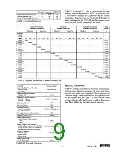
SPECIFICATIONS
All specifications at +25°C, +VCC = +VDD = +5V, fS = 44.1kHz, and 16-bit input data, SYSCLK = 384fS, unless otherwise noted.
PCM1721
PARAMETER
CONDITIONS
MIN
TYP
MAX
UNITS
RESOLUTION
16
24
Bits
DATA FORMAT
Audio Data Format
Data Bit Length
Standard/I2S
16/20/24
Selectable
44.1
Sampling Frequency (fS)
Standard fS
One-half fS
Double fS
32
16
64
48
24
96
kHz
kHz
kHz
22.05
88.2
PLL PERFORMANCE
Master Clock Input Frequency
Generated Sysclk Frequency
Generated Sysclk Jitter
27
MHz
256fS/384fS
fM = 27MHz
fM = 27MHz
±250
20
ps
ms
%
Generated Sysclk Transient(1)
Generated Sysclk Duty Cycle
fM = 27MHz, CL = 15pF
40
50
60
DIGITAL INPUT/OUTPUT LOGIC LEVEL
TTL
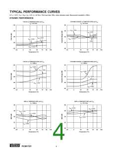
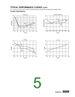
DYNAMIC PERFORMANCE(2)
THD+N at fS (0dB)
fs = 44.1kHz
fs = 96kHz
fs = 44.1kHz
fs = 96kHz
fs = 44.1kHz
fs = 96kHz
fs = 44.1kHz
fs = 96kHz
fs = 44.1kHz
–89
–87
–31
–29
94
–80
dB
dB
dB
dB
dB
dB
dB
dB
dB
THD+N at –60dB
Dynamic Range (EIAJ Method)
Signal-to-Noise Ratio(3)
Channel Separation
90
90
88
91
94
92
92
DC ACCURACY
Gain Error
±1.0
±1.0
±30
±5.0
±5.0
% of FSR
% of FSR
mV
Gain Mismatch, Channel-to-Channel
Bipolar Zero Error
VOUT = VCC/2 at BPZ
ANALOG OUTPUT
Output Voltage
Full Scale (–0dB)
AC Load
0.62 x VCC
VCC/2
Vp-p
VDC
kΩ
Center Voltage
Load Impedance
5
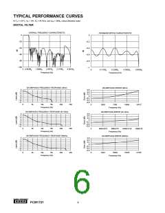
DIGITAL FILTER PERFORMANCE
Passband
0.445
fS
fS
Stopband
0.555
–35
Passband Ripple
Stopband Attenuation
Delay Time
±0.17
dB
dB
sec
dB
11.125/fS
De-emphasis Error
–0.2
+0.55
INTERNAL ANALOG FILTER
–3dB Bandwidth
100
kHz
dB
Passband Response
f = 20kHz
–0.16
POWER SUPPLY REQUIREMENTS
Voltage Range
VCC = VDD = VCP
fS = 44.1kHz
fS = 96kHz
4.5
5
5.5
43
58
VDC
mA
Supply Current: ICC + IDD + ICP
ICC + IDD + ICP
36
49
mA
TEMPERATURE RANGE
Operation
0
+70
°C
°C
Storage
–55
+100
NOTES: (1) Sysclk transient is the maximum frequency lock time when the PLL frequency is changed. (2) Dynamic performance specs are tested with 20kHz low
pass filter and THD+N specs are tested with 30kHz LPF, 400Hz HPF, Average-Mode. (3) SNR is tested at Infinite Zero Detection off.
The information provided herein is believed to be reliable; however, BURR-BROWN assumes no responsibility for inaccuracies or omissions. BURR-BROWN assumes no
responsibility for the use of this information, and all use of such information shall be entirely at the user’s own risk. Prices and specifications are subject to change without notice.
No patent rights or licenses to any of the circuits described herein are implied or granted to any third party. BURR-BROWN does not authorize or warrant any BURR-BROWN
product for use in life support devices and/or systems.
®
2
PCM1721

 BB [ BURR-BROWN CORPORATION ]