(a)
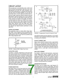
CIRCUIT LAYOUT
47kΩ
With any high-speed, wide-bandwidth circuitry, careful circuit
layout will ensure best performance. Make short, direct circuit
interconnections and avoid stray wiring capacitance—espe-
cially at the inverting input pin. A component-side ground plane
will help ensure low ground impedance. Do not place the
ground plane under or near the inputs and feedback network.
VO
CL
100pF
VI
G = 1
250pF
1kΩ
1kΩ
CL
CC
RC
(b)
100pF 10pF 20Ω
1000pF 47pF 20Ω
The power supply connections should be bypassed with good
high-frequency capacitors positioned close to the op amp pins.
In most cases, both a 1µF solid tantalum capacitor and a 0.1µF
ceramic capacitor are required on each supply. The OPA671
can deliver peak load currents up to 100mA. Even if steady-
state load currents are lower, signal transients may demand
large current transients from the power supplies. It is the power
supply bypass capacitors which must supply these current
transients. Larger bypass capacitors such as 4.7µF solid tanta-
lum capacitors may improve dynamic performance in some
applications.
CC
RC
VO
VI
CL
G = –1
1kΩ
1kΩ
(c)
330Ω
RC
VO
L ≤ 100pF
100pF
C
VI
G = –1
OFFSET ADJUSTMENT
See application bulletin AB-028 for
details on circuits for driving capacitive loads.
Many applications require no external offset voltage adjust-
ment. Figure 1 shows an optional circuit for trimming the offset
voltage. Do not use this offset voltage adjustment to correct for
offsets produced in other circuitry since this can introduce large
offset voltage temperature drift.
FIGURE 2. Compensation Circuits for Capacitive Loads.
assure that the maximum junction temperature is not exceeded.
The OPA671 may be operated at reduced power supply voltage
to minimize power dissipation.
V+
10kΩ
OUTPUT CURRENT LIMIT
5kΩ to 50kΩ
7
Potentiometer
1
Output current is limited by internal circuitry to approximately
90mA at 25°C. The short-circuit limit current decreases with
increasing junction temperature as shown in the typical curves.
The current limit will protect the device from inadvertent short-
circuits to ground. The internal power dissipation under this
condition, however, is quite high so short-circuits should be
avoided.
2
(10kΩ preferred)
5
OPA671
6
3
4
V–
FIGURE 1. Optional Offset Voltage Trim Circuit.
CAPACITIVE LOADS
INPUT BIAS CURRENT
The OPA671 is internally compensated to be unity-gain stable
with minimal capacitive load. The combination of low closed-
loop gain and capacitive load will decrease the phase margin
and may lead to gain peaking or oscillations. Load capacitance
reacts with the op amp’s open-loop output resistance to form an
additional pole in the feedback loop. With wideband op amps,
load capacitance as low as 50pF can introduce enough phase
shift to degrade dynamic performance. Figure 2 shows circuits
which preserve phase margin with capacitive load. Request
Application Bulletin AB-028 for details on various compensa-
tion circuits and analysis techniques.
The OPA671 is fabricated with Burr-Brown’s dielectrically
isolated Difet process, giving it extremely low input bias
current. As with other FET-input amplifiers, input bias current
approximately doubles with every 10°C increase in junction
temperature. Input bias current can be minimized by soldering
the device to the circuit board to provided best heat dissipation.
Reduced power supply voltage will also minimize input bias
current by reducing internal power dissipation.
DEMONSTRATION BOARD
The OPA671 may be evaluated using a high frequency PC
board developed for the OPA65x op amp family. This board
may be ordered from your local Burr-Brown distribution as part
# DEM-OPA65xP. It comes partially assembled but does not
include the amplifier. Since this board was intended for ±5V
amplifier, verify that any electrolytic capacitors loaded on the
board can support the higher supply voltages possible with the
OPA671.
POWER DISSIPATION
High output current can cause large internal power dissipation
in the OPA671. Copper leadframe construction improves heat
dissipation compared to conventional plastic packages. To
achieve best heat dissipation, solder the device directly to the
circuit board and use wide circuit board traces close to the
device pins. Limit the ambient temperature, load and signal to
®
7
OPA671

 BB [ BURR-BROWN CORPORATION ]