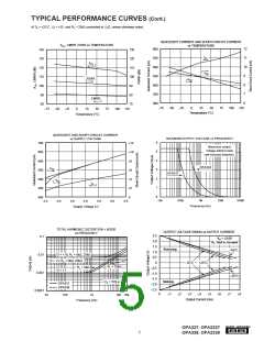
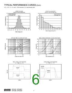
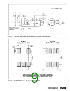
APPLICATIONS INFORMATION
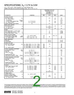
+5V
The OPA337 series and OPA338 series are fabricated on a
state-of-the-art CMOS process. The OPA337 series is unity-
gain stable. The OPA338 series is optimized for gains
greater than or equal to five. Both are suitable for a wide
range of general purpose applications. Power supply pins
should be bypassed with 0.01µF ceramic capacitors.
IOVERLOAD
10mA max
OPA337
VOUT
VIN
5kΩ
FIGURE 2. Input Current Protection for Voltages Exceeding
the Supply Voltage.
OPERATING VOLTAGE
The OPA337 series and OPA338 series can operate from a
+2.5V to +5.5V single supply with excellent performance.
Unlike most op amps which are specified at only one supply
voltage, these op amps are specified for real-world applica-
tions; a single limit applies throughout the +2.7V to +5.5V
supply range. This allows a designer to have the same
assured performance at any supply voltage within the speci-
fied voltage range. Most behavior remains unchanged
throughout the full operating voltage range. Parameters
which vary significantly with operating voltage are shown in
typical performance curves.
USING THE OPA338 IN LOW GAINS
The OPA338 series is optimized for gains greater than or
equal to five. It has significantly wider bandwidth (12.5MHz)
and faster slew rate (4.6V/µs) when compared to the OPA337
series. The OPA338 series can be used in lower gain con-
figurations at low frequencies while maintaining its high
slew rate with the proper compensation.
Figure 3 shows the OPA338 in a unity-gain buffer configu-
ration. At dc, the compensation capacitor C1 is effectively
“open” resulting in 100% feedback (closed-loop gain = 1).
As frequency increases, C1 becomes lower impedance and
closed-loop gain increases, eventually becoming 1 + R2/R1
(in this case five, which is equal to the minimum gain
required for stability).
OPA337, VIN = ±3V Greater Than VS = ±2.5V
VOUT, G = –1
(not limited by
3V
input common-
mode range.)
The required compensation capacitor value can be deter-
mined from the following equation:
C1 = 1/(2πfCR1)
0
Since fC may shift with process variations, it is recom-
mended that a value less than fC be used for determining C1.
With fC = 1MHz and R1 = 2.5kΩ, the compensation capaci-
tor is about 68pF.
G = ±1
VOUT, G = +1
(limited by input
common-mode
range)
–3V
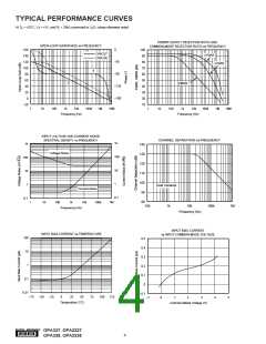
The selection of the compensation capacitor C1 is important.
A proper value ensures that the closed-loop circuit gain is
greater than or equal to five at high frequencies. Referring to
the “Open-Loop Gain vs Frequency” plot in the Typical
Performance Curves section, the OPA338 gain line (dashed
in the curve) has a constant slope (–20dB/decade) up to
approximately 3MHz. This frequency is referred to as fC.
Beyond fC the slope of the curve increases, suggesting that
closed-loop gains less than 5 are not appropriate.
FIGURE 1. OPA337—No Phase Inversion with Inputs
Greater than the Power Supply Voltage.
INPUT VOLTAGE
The input common-mode range extends from (V–) – 0.2V to
(V+) – 1.2V. For normal operation, inputs should be
limited to this range. The absolute maximum input voltage
is 500mV beyond the supplies. Inputs greater than the
input common-mode range but less than maximum input
voltage, while not valid, will not cause any damage to the
op amp. Furthermore, if input current is limited the inputs
may go beyond the power supplies without phase inver-
sion (Figure 1) unlike some other op amps.
Improved slew rate (4.6V/µs) versus
R2
OPA337 (1.2V/µs) in unity gain.
10kΩ
R1
2.5kΩ
C1
68pF
OPA338
VOUT
Normally, input currents are 0.2pA. However, large inputs
(greater than 500mV beyond the supply rails) can cause
excessive current to flow in or out of the input pins.
Therefore, as well as keeping the input voltage below the
maximum rating, it is also important to limit the input
current to less than 10mA. This is easily accomplished
with an input resistor as shown in Figure 2.
VIN
1
C1 =
2πfCR1
Where fC is the frequency at which closed-loop
gains less than five are not appropriate—see text.
FIGURE 3. Compensation of OPA338 for Unity-Gain Buffer.
®
OPA337, OPA2337
OPA338, OPA2338
7

 BB [ BURR-BROWN CORPORATION ]